# A B C D E F G H I J K L M N O P Q R S T U V W X Y Z

ST TL072, TL072A, TL072B Low Noise JFET Dual Operational Amplifiers Data Sheet

Summary

Explore the TL072 series, a robust dual operational amplifier featuring high-speed JFET inputs optimized for low noise and current draw. This component provides reliable analog signal amplification in demanding applications. The accompanying datasheet offers professional designers comprehensive technical specifications, including detailed electrical characteristics, operating limits, and absolute maximum ratings. It is essential documentation for engineers designing circuits that require precision, stability, and minimal offset current performance.
📄 Preview 📖 Table of Contents Contents PAGE OF 16

Page 1 Text Content

TL072, TL072A, TL072B

Low noise JFET dual operational amplifiers

Datasheet — production data

Features

+) and

Wide common-mode (up to VCC differential voltage range Low input bias and offset current Low noise en = 15 n V/√Hz (typ)

Output short-circuit protection DIP8 (Plastic package)

High input impedance JFET input stage Low harmonic distortion: 0.01% (typical) Internal frequency compensation Latch-up free operation High slew rate: 16 V/µs (typ)

(Plastic micropackage)

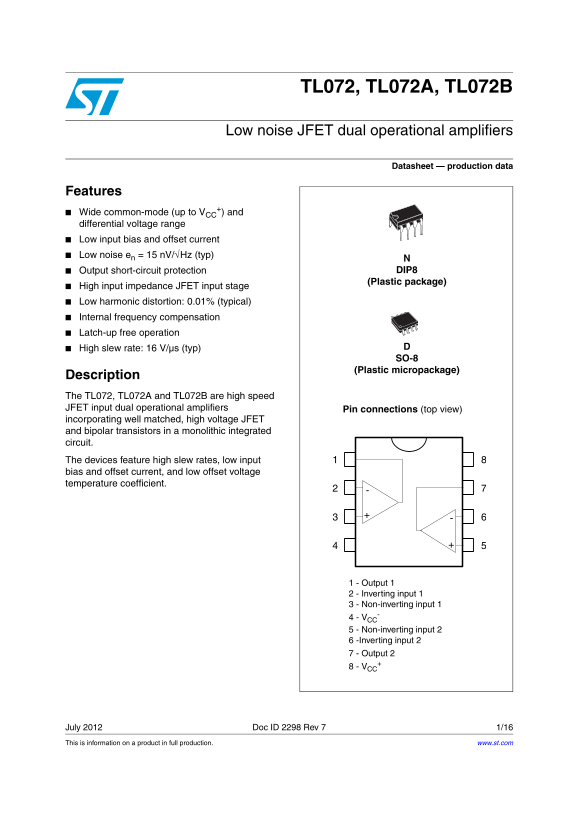
Description The TL072, TL072A and TL072B are high speed JFET input dual operational amplifiers Pin connections (top view) incorporating well matched, high voltage JFET and bipolar transistors in a monolithic integrated circuit. The devices feature high slew rates, low input bias and offset current, and low offset voltage temperature coefficient.

1 - Output 1 2 - Inverting input 1 3 - Non-inverting input 1 4 - VCC 5 - Non-inverting input 2 6 -Inverting input 2 7 - Output 2 8 - VCC

July 2012 Doc ID 2298 Rev 7 1/16 This is information on a product in full production. www.st.com

Page Summary Contents For ST TL072, TL072A, TL072B Low Noise JFET Dual Operational Amplifiers Data Sheet

Page 1 TL072, TL072A, TL072B Low noise JFET dual operational amplifiers Datasheet — production data Features +) and Wide common-mode (up to VCC differential voltage range Low input bias and offset current Lo...
Page 2 Schematic diagram TL072, TL072A, TL072B 1 Schematic diagram Figure 1. Schematic diagram Non- inver ting input Inverting input Output 1/2 TL07230k 2/16 Doc ID 2298 Rev 7
Page 3 TL072, TL072A, TL072B Absolute maximum ratings and operating conditions 2 Absolute maximum ratings and operating conditions Table 1. Absolute maximum ratings TL072C, AC, Symbol Parameter TL072I, AI, B...
Page 4 Electrical characteristics TL072, TL072A, TL072B 3 Electrical characteristics Table 3. Electrical characteristics at VCC = ±15V, Tamb = +25°C (unless otherwise specified) TL072I,AC,AI TL072C BC,BI Sym...
Page 5 TL072, TL072A, TL072B Electrical characteristics Table 3. Electrical characteristics at VCC = ±15V, Tamb = +25°C (unless otherwise specified) (continued) TL072I,AC,AI TL072C BC,BI Symbol Parameter Uni...
Page 6 Electrical characteristics TL072, TL072A, TL072B Figure 2. Maximum peak-to-peak output Figure 3. Maximum peak-to-peak output voltage versus frequency (RL= 2kΩ) voltage versus frequency (RL= 10kΩ) Figu...
Page 7 TL072, TL072A, TL072B Electrical characteristics SU PP LY UR EN (m A) IN PU BI AS EN (n A) Figure 8. Input bias current versus free air Figure 9. Large signal differential voltage temperature amplific...
Page 8 Electrical characteristics TL072, TL072A, TL072B EQ IV AL EN IN PU NO IS VO LT AG (n V/ VH z) Figure 14. Voltage follower large signal pulse Figure 15. Output voltage versus elapsed time response OVER...
Page 9 TL072, TL072A, TL072B Parameter measurement information 4 Parameter measurement information Figure 18. Voltage follower Figure 19. Gain-of-10 inverting amplifier TL072 RL CL= 100p F Doc ID 2298 Rev 7 ...
Page 10 Typical application TL072, TL072A, TL072B 5 Typical application Figure 20. k Hz quadruple oscillator -TL072 88.4k Ω 6 cos ω t TL072 6 sin ω t * These resistor values may be adjusted for a symmetrical ...
Page 11 TL072, TL072A, TL072B Package information 6 Package information In order to meet environmental requirements, ST offers these devices in different grades of ECOPACK® packages, depending on their level ...
Page 12 Package information TL072, TL072A, TL072B 6.1 DIP8 package information Figure 21. DIP8 package mechanical drawing Table 4. DIP8 package mechanical data Dimensions Ref. Millimeters Inches Min. Typ. Max...
Page 13 TL072, TL072A, TL072B Package information 6.2 SO-8 package information Figure 22. SO-8 package mechanical drawing Table 5. SO-8 package mechanical data Dimensions Ref. Millimeters Inches Min. Typ. Max...
Page 14 Ordering information TL072, TL072A, TL072B 7 Ordering information Table 6. Order codes Order code Temperature range Package Packing Marking TL072IN TL072IN TL072AIN DIP8 Tube TL072AIN TL072BIN TL072BI...
Page 15 TL072, TL072A, TL072B Revision history 8 Revision history Table 7. Document revision history Date Revision Changes 28-Mar-2001 Initial release. 02-Apr-2004 Correction to pin connection diagram on cove...
Page 16 TL072, TL072A, TL072B Please Read Carefully: Information in this document is provided solely in connection with ST products. STMicroelectronics NV and its subsidiaries (“ST”) reserve the right to make...