ST TS27M2C, I, M PRECISION LOW POWER CMOS DUAL OPERATIONAL AMPLIFIERS Data Sheet
Summary
These ultra-low power CMOS dual operational amplifiers are ideal for demanding, space-constrained analog circuits requiring high efficiency and stability. The TS27 series provides optimized consumption/speed ratios, operating with single or dual supplies while maintaining excellent phase margin. This comprehensive manual details detailed electrical characteristics, ensuring users can select the optimal low-power variant (10µA to 150µA) for their designs. Perfect for electronics engineers developing battery-powered medical instrumentation, IoT devices, and precision analog measurement systems.
Page 1 Text Content
查询TS27M2AC供应商
TS27M2C,I,M PRECISION LOW POWER
CMOS DUAL OPERATIONAL AMPLIFIERS
LOW POWER CONSUMPTION : 150µA/op OUTPUT VOLTAGE CAN SWING TO GROUND EXCELLENT PHASE MARGIN ON CAPACITIVE LOADS STABLE AND LOW OFFSET VOLTAGE
DIP8 (Plastic Package)
THREE INPUT OFFSET VOLTAGE SELECTIONS
DESCRIPTION
These devices are low cost, low power dual oper-
ational amplifiers designed to operate with single
(Plastic Micropackage)
or dual supplies. These operational amplifiers use the ST silicon gate CMOS process allowing an ex- cellent consumption-speed ratio. These series are ideally suited for low consumption applications.
Three power consumptions are available allowing
TSSOP8
to have always the best consumption-speed ratio:
(Thin Shrink Small Outline Package)
ICC = 10µA/amp.: TS27L2 (very low power)
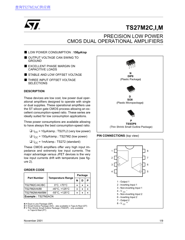
PIN CONNECTIONS (top view)
ICC = 150µA/amp.: TS27M2 (low power) ICC = 1m A/amp.: TS272 (standard) These CMOS amplifiers offer very high input im- pedance and extremely low input currents. The major advantage versus JFET devices is the very low input currents drift with temperature (see fig- ure 2).
ORDER CODE
Package
Part Number Temperature Range
1 - Output 1 TS27M2C/AC/BC 0°C, +70°C 2 - Inverting Input 1 3 - Non-inverting Input 1
TS27M2I/AI/BI -40°C, +125°C
4 - V CC
TS27M2M/AM/BM -55°C, +125°C
5 - Non-inverting Input 2
Example : TS27M2ACN
6 - Inverting Input 2 7 - Output 2 N = Dual in Line Package (DIP) 8 - V CC
D = Small Outline Package (SO) - also available in Tape & Reel (DT) P = Thin Shrink Small Outline Package (TSSOP) - only available in Tape & Reel (PT)
November 2001 1/9
Page Summary Contents For ST TS27M2C, I, M PRECISION LOW POWER CMOS DUAL OPERATIONAL AMPLIFIERS Data Sheet
Manual Details
| Brand | Dual |
|---|---|
| Pages | 10 |
| File Size | 94.76 KB |
| Published | June 03, 2026 |
Enter the captcha to get the download link:
