ST TS272C, I, M High Performance CMOS Dual Operational Amplifiers Data Sheet/Manual
Summary
Discover the TS272 series of low-cost, high-performance CMOS dual operational amplifiers. These ultra-reliable op-amps are engineered for power-sensitive applications requiring excellent stability and minimal current draw across a wide temperature range (-55°C to +125°C). This comprehensive manual provides all essential technical specifications, including operating conditions, electrical characteristics (e.g., high CMRR, low output offset), and detailed package information in DIP, SO, and TSSOP formats. Ideal for engineers designing precision analog circuits or portable electronic devices seeking maximum efficiency with industry-leading performance-to-power ratio.
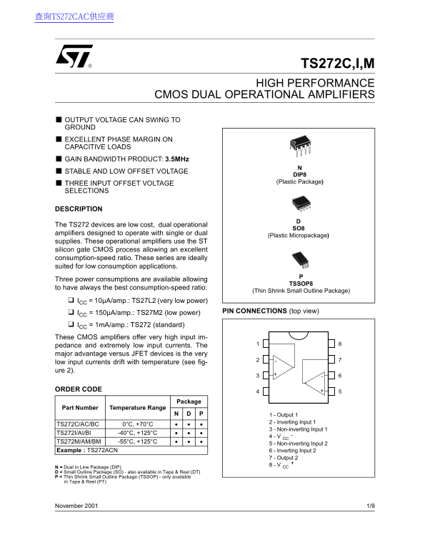
Page 1 Text Content
查询TS272CAC供应商
TS272C,I,M HIGH PERFORMANCE
CMOS DUAL OPERATIONAL AMPLIFIERS
OUTPUT VOLTAGE CAN SWING TO GROUND EXCELLENT PHASE MARGIN ON CAPACITIVE LOADS GAIN BANDWIDTH PRODUCT: 3.5MHz STABLE AND LOW OFFSET VOLTAGE
DIP8 (Plastic Package)
THREE INPUT OFFSET VOLTAGE SELECTIONS
DESCRIPTION
The TS272 devices are low cost, dual operational
amplifiers designed to operate with single or dual
(Plastic Micropackage)
supplies. These operational amplifiers use the ST silicon gate CMOS process allowing an excellent consumption-speed ratio. These series are ideally suited for low consumption applications.
Three power consumptions are available allowing
TSSOP8
to have always the best consumption-speed ratio:
(Thin Shrink Small Outline Package)
ICC = 10µA/amp.: TS27L2 (very low power)
PIN CONNECTIONS (top view)
ICC = 150µA/amp.: TS27M2 (low power) ICC = 1m A/amp.: TS272 (standard) These CMOS amplifiers offer very high input im- pedance and extremely low input currents. The major advantage versus JFET devices is the very low input currents drift with temperature (see fig- ure 2).
ORDER CODE
Package
Part Number Temperature Range
1 - Output 1 2 - Inverting Input 1
TS272C/AC/BC 0°C, +70°C
3 - Non-inverting Input 1
TS272I/AI/BI -40°C, +125°C
4 - V CC
TS272M/AM/BM -55°C, +125°C
5 - Non-inverting Input 2
Example : TS272ACN 6 - Inverting Input 2
7 - Output 2 8 - V N = Dual in Line Package (DIP) CC
D = Small Outline Package (SO) - also available in Tape & Reel (DT) P = Thin Shrink Small Outline Package (TSSOP) - only available in Tape & Reel (PT)
November 2001 1/9
Page Summary Contents For ST TS272C, I, M High Performance CMOS Dual Operational Amplifiers Data Sheet/Manual
Manual Details
| Brand | Dual |
|---|---|
| Pages | 9 |
| File Size | 128.15 KB |
| Published | June 03, 2026 |
Enter the captcha to get the download link:

Frequently Asked Questions
What is the maximum Gain Bandwidth Product (GBP)?
The typical Gain Bandwidth Product is 3.5 MHz for all variants.
Which operational amplifier variant supports temperatures from -40°C to +125°C?
The TS272I/AI/BI models operate reliably in the temperature range of -40°C to +125°C.
Are there different power modes for the amplifiers?
Yes, three consumption levels are available: TS27L2 (very low power), TS27M2 (low power), and TS272 (standard).