ST TS27L4C, I, M PRECISION VERY LOW POWER CMOS QUAD OPERATIONAL AMPLIFIER Data Sheet
Summary
These ultra low-power quad operational amplifiers, featuring a CMOS design and excellent power consumption/speed ratio, are ideal for battery-operated and minimal-power applications. The manual provides comprehensive documentation, including operating characteristics, detailed electrical specifications, and reliable data across various temperature grades (-40°C to +125°C). Designed for hardware designers seeking stable, low-offset circuitry with high input impedance, it supports single or dual power supplies in multiple packages (DIP/TSSOP).
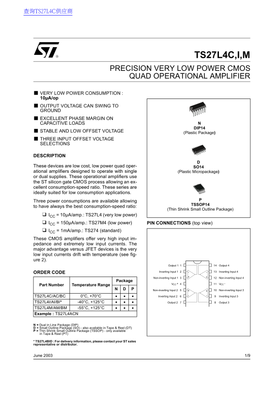
Page 1 Text Content
查询TS27L4C供应商
TS27L4C,I,M
PRECISION VERY LOW POWER CMOS QUAD OPERATIONAL AMPLIFIER
VERY LOW POWER CONSUMPTION : 10µA/op OUTPUT VOLTAGE CAN SWING TO GROUND EXCELLENT PHASE MARGIN ON CAPACITIVE LOADS
DIP14
STABLE AND LOW OFFSET VOLTAGE
(Plastic Package)
THREE INPUT OFFSET VOLTAGE SELECTIONS
DESCRIPTION
These devices are low cost, low power quad oper- SO14 ational amplifiers designed to operate with single (Plastic Micropackage) or dual supplies. These operational amplifiers use the ST silicon gate CMOS process allowing an ex- cellent consumption-speed ratio. These series are ideally suited for low consumption applications.
Three power consumptions are available allowing
TSSOP14
to have always the best consumption-speed ratio:
(Thin Shrink Small Outline Package)
ICC = 10µA/amp.: TS27L4 (very low power) ICC = 150µA/amp.: TS27M4 (low power) PIN CONNECTIONS (top view) ICC = 1m A/amp.: TS274 (standard) These CMOS amplifiers offer very high input im- pedance and extremely low input currents. The major advantage versus JFET devices is the very low input currents drift with temperature (see fig- ure 2).
Output 1 Output 4
Inverting Input 1 Inverting Input 4
ORDER CODE
Non-inverting Input 1 Non-inverting Input 4
Package
CCV -CCV
Part Number Temperature Range
Non-inverting Input 2 Non-inverting Input 3
TS27L4C/AC/BC 0°C, +70°C Inverting Input 2 Inverting Input 3
TS27L4I/AI/BI* -40°C, +125°C Output 2 Output 3 TS27L4M/AM/BM -55°C, +125°C Example : TS27L4ACN
N = Dual in Line Package (DIP) D = Small Outline Package (SO) - also available in Tape & Reel (DT) P = Thin Shrink Small Outline Package (TSSOP) - only available in Tape & Reel (PT)
* TS27L4BID : For delivery information, please contact your ST sales representative or distributor.
June 2003 1/9
Page Summary Contents For ST TS27L4C, I, M PRECISION VERY LOW POWER CMOS QUAD OPERATIONAL AMPLIFIER Data Sheet
Manual Details
| Brand | QUAD |
|---|---|
| Pages | 10 |
| File Size | 104.34 KB |
| Published | June 04, 2026 |
Enter the captcha to get the download link:

Frequently Asked Questions
What is the main advantage of using this CMOS amplifier technology?
These amplifiers offer very high input impedance and extremely low input currents that do not drift with temperature.
What are the available operating current options for these amps?
Three power consumption versions are available: TS27L4 at 10μA/amp, TS27M4 at 150μA/amp, and TS274 at 1mA/amp.
What is the maximum allowable supply voltage?
The absolute maximum rating for the supply voltage (V CC) is 18 V.
Can this amplifier operate in extreme temperatures?
Yes; specific variants are rated for extended ranges, such as -40°C to +125°C or -55°C to +125°C.