# A B C D E F G H I J K L M N O P Q R S T U V W X Y Z

ST LM124, LM224, LM324 Low Power Quad Operational Amplifiers Datasheet

Summary

These low-power quad operational amplifiers are essential components for demanding signal processing applications. Featuring high gain, wide bandwidth, and exceptionally low supply current, they offer versatile operation from both single and dual power supplies. The comprehensive manual provides detailed specifications, pin configurations, timing characteristics, and application guidelines necessary for integration into complex electronic designs. Ideal for engineers designing sensitive or power-constrained circuits requiring precision amplification performance.
📄 Preview 📖 Table of Contents Contents PAGE OF 19

Page 1 Text Content

LM124, LM224, LM324

Low power quad operational amplifiers

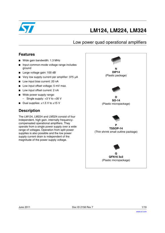
Features Wide gain bandwidth: 1.3 MHz Input common-mode voltage range includes ground

Large voltage gain: 100 d B DIP14 (Plastic package)

Very low supply current per amplifier: 375 µA Low input bias current: 20 n A Low input offset voltage: 5 m V max. Low input offset current: 2 n A Wide power supply range: Single supply: +3 V to +30 V

SO-14

Dual supplies: ±1.5 V to ±15 V

(Plastic micropackage)

Description The LM124, LM224 and LM324 consist of four independent, high gain, internally frequency- compensated operational amplifiers. They operate from a single power supply over a wide

TSSOP-14

range of voltages. Operation from split power

(Thin shrink small outline package)

supplies is also possible and the low power supply current drain is independent of the magnitude of the power supply voltage.

QFN16 3x3 (Plastic micropackage)

June 2011 Doc ID 2156 Rev 7 1/19

www.st.com

Page Summary Contents For ST LM124, LM224, LM324 Low Power Quad Operational Amplifiers Datasheet

Page 1 LM124, LM224, LM324 Low power quad operational amplifiers Features Wide gain bandwidth: 1.3 MHz Input common-mode voltage range includes ground Large voltage gain: 100 d B DIP14 (Plastic package) Very...
Page 2 Pin and schematic diagram LM124, LM224, LM324 1 Pin and schematic diagram Figure 1. Pin connections (top view) Output Output Inverting Input Inverting Input Non-inverting Input Non-inverting Input Non...
Page 3 LM124, LM224, LM324 Absolute maximum ratings 2 Absolute maximum ratings Table 1. Absolute maximum ratings Symbol Parameter LM124 LM224 LM324 Unit VCC Supply voltage ±16 or 32 Vin Input voltage(1) -0.3...
Page 4 Electrical characteristics LM124, LM224, LM324 3 Electrical characteristics + = +5 V, VCC -= ground, Vo = 1.4 V, Tamb = +25° C (unless otherwise Table 2. VCC specified) Symbol Parameter Min. Typ. Max....
Page 5 LM124, LM224, LM324 Electrical characteristics + = +5 V, VCC -= ground, Vo = 1.4 V, Tamb = +25° C (unless otherwise Table 2. VCC specified) (continued) Symbol Parameter Min. Typ. Max. Unit Output sink...
Page 6 Electrical characteristics LM124, LM224, LM324 Figure 3. Input bias current vs. ambient ai ba nd id th ro du ct z) Figure 4. Current limiting temperature In vo lta IB (n A) Ambient temperature (°C) Te...
Page 7 LM124, LM224, LM324 Electrical characteristics Figure 9. Open loop frequency response Figure 10. Large signal frequency response ol ta ge ai (d In pu t v ol ta ge ou tp ut ol ta ge ut pu t v ol ta ge ...
Page 8 Electrical characteristics LM124, LM224, LM324 Figure 15. Input current Figure 16. Large signal voltage gain ow er up pl om on od re je ct io ra tio d B Avd (d B) In rr (n Tamb = +25°C Power supply vo...
Page 9 LM124, LM224, LM324 Typical single-supply applications 4 Typical single-supply applications Figure 19. AC coupled inverting amplifier Figure 20. High input Z adjustable gain DC instrumentation amplifi...
Page 10 Typical single-supply applications LM124, LM224, LM324 Figure 25. Active bandpass filter Figure 26. High input Z, DC differential amplifier R1 R4 For R2 R3 (CMRR depends on this resistor ratio match) ...
Page 11 LM124, LM224, LM324 Package information 5 Package information In order to meet environmental requirements, ST offers these devices in different grades of ECOPACK® packages, depending on their level of...
Page 12 Package information LM124, LM224, LM324 5.1 DIP14 package information Figure 28. DIP14 package mechanical drawing Table 3. DIP14 package mechanical data Dimensions Millimeters Inches Min. Typ. Max. Mi...
Page 13 LM124, LM224, LM324 Package information 5.2 SO-14 package information Figure 29. SO-14 package mechanical drawing Table 4. SO-14 package mechanical data Dimensions Millimeters Inches Min. Typ. Max. Mi...
Page 14 Package information LM124, LM224, LM324 5.3 QFN16 3x3 package mechanical data Figure 30. QFN16 3x3 package mechanical drawing 14/19 Doc ID 2156 Rev 7
Page 15 LM124, LM224, LM324 Package information Table 5. QFN16 3x3 mm package mechanical data (pitch 0.5 mm) Dimensions Ref. Millimeters Inches Min. Typ. Max. Min. Typ. Max. Figure 31. QFN16 3x3 footprint rec...
Page 16 Package information LM124, LM224, LM324 5.4 TSSOP14 package information Figure 32. TSSOP14 package mechanical drawing Figure 33. TSSOP14 package mechanical data Dimensions Ref. Millimeters Inches Min....
Page 17 LM124, LM224, LM324 Ordering information 6 Ordering information Table 6. Order codes Part number Temperature range Package Packing Marking LM124N DIP14 Tube LM124N LM124D/DT SO-14 Tube or tape & r...
Page 18 Revision history LM124, LM224, LM324 7 Revision history Table 7. Document revision history Date Revision Changes 01-Oct.-2003 First release. Modifications on AMR Table 1 on page 3 (explanation of Vid ...
Page 19 LM124, LM224, LM324 Please Read Carefully: Information in this document is provided solely in connection with ST products. STMicroelectronics NV and its subsidiaries (“ST”) reserve the right to make c...

Manual Details

Brand QUAD
Pages 19
File Size 1.36 MB
Published June 04, 2026
52 views

Enter the captcha to get the download link:

captcha

Frequently Asked Questions

What power supply ranges are supported by these amplifiers?

They support both single supplies (+3 V to +30 V) and split supplies (±1.5 V to ±15 V).

What safety precautions should I take concerning short circuits?

Short-circuits can cause excessive heating, and simultaneous short-circuiting on all amplifiers can result in destructive dissipation.

How should an input driven negative be protected?

The junction base/substrate of the input PNP transistor must be protected by a resistor in series with the inputs to limit current (R = (Vin - 32 V)/400 µA).

What is the typical input bias current?

At room temperature, the typical input bias current is 20 nA.