ST L272 July 2003 DUAL POWER OPERATIONAL AMPLIFIERS
Summary
The L272 is a robust dual power operational amplifier engineered for demanding applications requiring high output current capability (up to 1A) and reliability across single or split low-voltage supplies. Ideal for engineers building automation, servo, and motor speed control circuits, this integrated circuit features ground-compatible inputs and excellent Common Mode Rejection. The comprehensive manual provides detailed technical specifications, thermal data, electrical performance graphs, and multiple application suggestions necessary for robust system design in professional electronics.
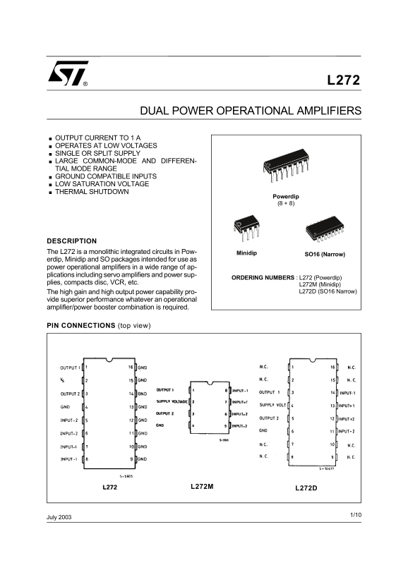
Page 1 Text Content
DUAL POWER OPERATIONAL AMPLIFIERS
.OUTPUT CURRENT TO 1 A.OPERATES AT LOW VOLTAGES.SINGLE OR SPLIT SUPPLY.LARGE COMMON-MODE AND DIFFEREN- TIAL MODE RANGE.GROUND COMPATIBLE INPUTS.LOW SATURATION VOLTAGE.THERMAL SHUTDOWN
Powerdip (8 + 8)
DESCRIPTION The L272 is a monolithic integrated circuits in Pow- Minidip
SO16 (Narrow)
erdip, Minidip and SO packages intended for use as power operational amplifiers in a wide range of ap- plications including servo amplifiers and power sup-
ORDERING NUMBERS : L272 (Powerdip)
plies, compacts disc, VCR, etc.
L272M (Minidip) The high gain and high output power capability pro- L272D (SO16 Narrow)
vide superior performance whatever an operational amplifier/power booster combination is required.
PIN CONNECTIONS (top view)
L272DL272M
July 2003
Page Summary Contents For ST L272 July 2003 DUAL POWER OPERATIONAL AMPLIFIERS
Manual Details
| Brand | Dual |
|---|---|
| Pages | 10 |
| File Size | 892.28 KB |
| Published | June 05, 2026 |
Enter the captcha to get the download link:

Frequently Asked Questions
What is the maximum continuous output current?
The device can handle an Ido of 1 A.
Does the L272 support split or single supply operation?
Yes, it supports both single and split supplies.
What are the recommendations for ensuring circuit stability?
A 100nF capacitor corrected between supply pins is recommended to avoid instability.
What is the thermal shutdown junction temperature for L272?
Thermal Shutdown occurs at 145°C.