AD600/AD602: Dual, Low Noise, Wideband Variable Gain Amplifiers Data Handbook Specifications Owner's Manual
Summary
These dual-channel, low-noise variable gain amplifiers are designed for demanding signal processing applications that require highly accurate and stable amplification. Featuring independent channel control, precise variable attenuators, and ultra-low input noise, the units deliver exceptional performance across various frequencies. The comprehensive manual details the functional block diagram, extensive operating specifications, multiple temperature grades (including military standard versions), and application guides tailored for critical fields such as Ultrasound/Sonar imaging, RF communication systems, and high-performance signal measurement equipment.
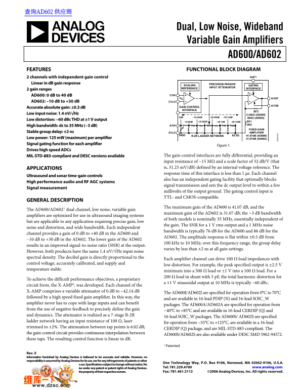
Page 1 Text Content
查询AD602 供应商
Dual, Low Noise, Wideband Variable Gain Amplifiers
AD600/AD602
FEATURES FUNCTIONAL BLOCK DIAGRAM
2 channels with independent gain control GAT1
Linear in d B gain response PRECISION PASSIVE
SCALING GATING
INPUT ATTENUATOR
REFERENCE INTERFACE
2 gain ranges
AD600: 0 d B to 40 d B C1HI VG A1OP
AD602: –10 d B to +30 d B C1LO
Accurate absolute gain: ±0.3 d B GAIN CONTROL INTERFACE
Low input noise: 1.4 n V/√Hz 2.24kΩ (AD600)
0d B –12.04d B –22.08d B –36.12d B 694Ω (AD602)
Low distortion: −60 d Bc THD at ±1 V output
–6.02d B –18.06d B –30.1d B –42.14d B RF1
A1HI 20Ω
High bandwidth: dc to 35 MHz (−3 d B)
FIXED-GAIN
Stable group delay: ±2 ns A1LO AMPLIFIER
500Ω R-2R LADDER NETWORK 62.5Ω 41.07d B (AD600)
Low power: 125 m W (maximum) per amplifier 31.07d B (AD602) Signal gating function for each amplifier
Figure 1.
Drives high speed ADCs
MIL-STD-883-compliant and DESC versions available The gain-control interfaces are fully differential, providing an input resistance of ~15 MΩ and a scale factor of 32 d B/V (that APPLICATIONS is, 31.25 m V/d B) defined by an internal voltage reference. The response time of this interface is less than 1 μs. Each channel
Ultrasound and sonar time-gain controls
also has an independent gating facility that optionally blocks
High performance audio and RF AGC systems
signal transmission and sets the dc output level to within a few
Signal measurement
millivolts of the output ground. The gating control input is TTL- and CMOS-compatible.
GENERAL DESCRIPTION
The maximum gain of the AD600 is 41.07 d B, and the
The AD600/AD6021 dual channel, low noise, variable gain
maximum gain of the AD602 is 31.07 d B; the −3 d B bandwidth
amplifiers are optimized for use in ultrasound imaging systems
of both models is nominally 35 MHz, essentially independent of
but are applicable to any application requiring precise gain, low
the gain. The SNR for a 1 V rms output and a 1 MHz noise
noise and distortion, and wide bandwidth. Each independent
bandwidth is typically 76 d B for the AD600 and 86 d B for the
channel provides a gain of 0 d B to +40 d B in the AD600 and
AD602. The amplitude response is flat within ±0.5 d B from
−10 d B to +30 d B in the AD602. The lower gain of the AD602
100 k Hz to 10 MHz; over this frequency range, the group delay
results in an improved signal-to-noise ratio (SNR) at the output.
varies by less than ±2 ns at all gain settings.
However, both products have the same 1.4 n V/√Hz input noise spectral density. The decibel gain is directly proportional to the
Each amplifier channel can drive 100 Ω load impedances with
control voltage, accurately calibrated, and supply and
low distortion. For example, the peak specified output is ±2.5 V
temperature stable.
minimum into a 500 Ω load or ±1 V into a 100 Ω load. For a 200 Ω load in shunt with 5 p F, the total harmonic distortion for 8-
To achieve the difficult performance objectives, a proprietary
a ±1 V sinusoidal output at 10 MHz is typically −60 d Bc.
circuit form, the X-AMP®, was developed. Each channel of the X-AMP comprises a variable attenuator of 0 d B to −42.14 d B
The AD600J/AD602J are specified for operation from 0°C to 70°C
followed by a high speed fixed gain amplifier. In this way, the
and are available in 16-lead PDIP (N) and 16-lead SOIC_W
amplifier never has to cope with large inputs and can benefit
packages. The AD600A/AD602A are specified for operation from
from the use of negative feedback to precisely define the gain
−40°C to +85°C and are available in 16-lead CERDIP (Q) and
and dynamics. The attenuator is realized as a 7-stage R-2R
16-lead SOIC_W packages. The AD600S/ AD602S are specified
ladder network having an input resistance of 100 Ω, laser
for operation from −55°C to +125°C, are available in a 16-lead
trimmed to ±2%. The attenuation between tap points is 6.02 d B;
CERDIP (Q) package, and are MIL-STD-883-compliant. The
the gain-control circuit provides continuous interpolation between
AD600S/AD602S are also available under DESC SMD 5962-94572.
these taps. The resulting control function is linear in d B.
1 Patented.
Rev. E Information furnished by Analog Devices is believed to be accurate and reliable. However, no responsibility is assumed by Analog Devices for its use, nor for any infringements of patents or other
One Technology Way, P.O. Box 9106, Norwood, MA 02062-9106, U.S.A.
rights of third parties that may result from its use. Specifications subject to change without notice. No
license is granted by implication or otherwise under any patent or patent rights of Analog Devices. Tel: 781.329.4700 www.analog.com Trademarks and registered trademarks are the property of their respective owners. Fax: 781.461.3113 ©2006 Analog Devices, Inc. All rights reserved.
Page Summary Contents For AD600/AD602: Dual, Low Noise, Wideband Variable Gain Amplifiers Data Handbook Specifications Owner's Manual
Manual Details
| Brand | Dual |
|---|---|
| Pages | 28 |
| File Size | 462.63 KB |
| Published | June 01, 2026 |
Enter the captcha to get the download link:

Frequently Asked Questions
What is the maximum nominal bandwidth for these amplifiers?
The models generally share a nominal -3 dB bandwidth of up to 35 MHz.
How is the gain setting controlled and how accurate is it?
Gain is set via fully differential interfaces, offering a linear response in decibels (dB) with an absolute gain accuracy of ±0.3 dB.
What applications are these variable gain amplifiers optimized for?
They are widely used in ultrasound and sonar time-gain control, high performance audio, and RF AGC systems.
What temperature ranges can users expect to choose from?
Available grades span commercial (0°C to 70°C) up to enhanced military specifications handling -55°C to +125°C, and some versions cover -55°C to +150°C.