National Semiconductor LMH6502 Wideband, Low Power, Linear-in-dB Variable Gain Amplifier Data Sheet
Summary
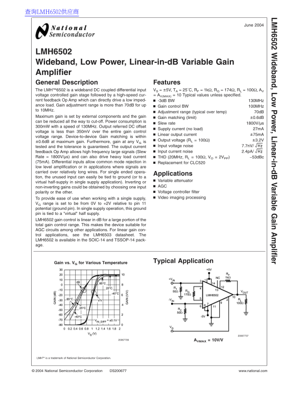
The LMH6502 is a high-performance, ultra-low power variable gain amplifier designed for demanding signal conditioning tasks. Featuring a wideband bandwidth up to 130MHz and a linear-in-dB gain control range exceeding 70dB, this device excels at maintaining accuracy in complex analog circuits. The manual provides comprehensive specifications for differential and single-supply operation, making it ideal for engineers developing video processing systems or automatic gain control (AGC) circuitry requiring high speed and precision amplification.
Page 1 Text Content
查询LMH6502供应商
LM ideband,Low ow er,Linear-in-d B Variable ain plifier
LMH6502 Wideband, Low Power, Linear-in-d B Variable Gain Amplifier General Description Features
The LMH™6502 is wideband DC coupled differential input VS ±5V, TA 25˚C, RF 1kΩ, RG 174Ω, RL 100Ω, AV voltage controlled gain stage followed by high-speed cur- AV(MAX) Typical values unless specified.
rent feedback Op Amp which can directly drive low imped- -3d B BW 130MHz ance load. Gain adjustment range is more than 70d B for up
Gain control BW 100MHz
to 10MHz.
Adjustment range (typical over temp) 70d B
Maximum gain is set by external components and the gain ±0.6d B
Gain matching (limit)
can be reduced all the way to cut-off. Power consumption is
Slew rate 1800V/µs
300m W with speed of 130MHz. Output referred DC offset
Supply current (no load) 27m A
voltage is less than 350m V over the entire gain control
Linear output current ±75m A
voltage range. Device-to-device Gain matching is within
Output voltage (RL 100Ω) ±3.2V
±0.6d B at maximum gain. Furthermore, gain at any VG is
tested and the tolerance is guaranteed. The output current Input voltage noise 7.7n V/ feedback Op Amp allows high frequency large signals (Slew Input current noise 2.4p A/
Rate 1800V/µs) and can also drive heavy load current THD (20MHz, RL 100Ω, VO 2VPP) −53d Bc (75m A). Differential inputs allow common mode rejection in Replacement for CLC520 low level amplification or in applications where signals are carried over relatively long wires. For single ended opera-
Applications
tion, the unused input can easily be tied to ground (or to
Variable attenuator
virtual half-supply in single supply application). Inverting or
non-inverting gains could be obtained by choosing one input AGC polarity or the other. Voltage controller filter To provide ease of use when working with single supply, Video imaging processing
VG range is set to be from 0V to +2V relative to pin potential (ground pin). In single supply operation, this ground pin is tied to "virtual" half supply. LMH6502 gain control is linear in d B for large portion of the total gain control range. This makes the device suitable for AGC circuits among other applications. For linear gain con- trol applications, see the LMH6503 datasheet. The LMH6502 is available in the SOIC-14 and TSSOP-14 pack- age.
Typical Application
Gain vs. VG for Various Temperature
AVMAX 10V/V
LMH™ is trademark of National Semiconductor Corporation.
National Semiconductor Corporation DS200677 www.national.com
Page Summary Contents For National Semiconductor LMH6502 Wideband, Low Power, Linear-in-dB Variable Gain Amplifier Data Sheet
Manual Details
| Brand | National |
|---|---|
| Pages | 19 |
| File Size | 920.85 KB |
| Published | June 05, 2026 |
Enter the captcha to get the download link:

Frequently Asked Questions
What is the total variable gain adjustment range available?
The gain adjustment range for this amplifier is more than 70dB.
How does the device handle single power supply environments?
It supports single supply by setting the voltage range from 0V to +2V relative to pin 11, treating the ground pin as a virtual half-supply.
Is common mode rejection possible with differential inputs?
Yes, the differential inputs allow for robust common mode rejection.
What is the operational bandwidth and slew rate?
The -3dB bandwidth ranges from 10MHz to 130MHz, and it features a high slew rate of 1800V/µs.