National Semiconductor CLC5506 Gain Trim Amplifier (GTA) Data Sheet
Summary
The CLC5506 is a high-performance, low-noise gain trim amplifier designed for robust programmable signal amplification across demanding RF/IF subsystems. Providing up to 600MHz bandwidth and compensating for system variations, this component allows precise gain control vital for advanced receiver front ends. The manual details its electrical specifications, operational parameters (spanning -40°C to +85°C), digital interface using MICROWIRE™, and high-output drive capabilities. It is ideally suited for communication professionals developing equipment for cellular base stations, radar systems, wireless local loops, and IF receivers.
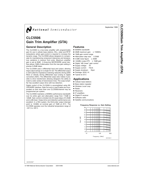
Page 1 Text Content
LC 5506G ain Trim plifier (G TA
September
CLC5506 Gain Trim Amplifier (GTA) General Description Features
The CLC5506 is low-noise amplifier with programmable 600MHz bandwidth
gain for use in cellular stations, WLL, radar and RF/IF 26d B maximum gain 150MHz subsystems where gain-control is required to increase the 16d B gain control range dynamic range. The CLC5506 allows designers to compen- Attenuation step size: 0.25d B sate for manufacturing component tolerances and tempera-
4.8d B noise figure 26d B
ture variations in receiver ends. Maximum amplifier
+22d Bm output IP3 18d B gain
gain is set at 26d B three-line MICROWIRE serial inter-
Digital ″d B Linear″ gain control
face allows 16d B of attenuation from the max gain setting in
Supply voltage: 5V
precise 0.25d B steps.
Supply current: 75m A
The CLC5506 uses differential input and output, allowing
Supply shutdown: 35µA
large output swings on single 5V rail. The differential output
is well suited for impedance matching networks driving SAW Package: SOIC-14 filters or directly driving differential input analog to digital Typical at 25˚C
converters (ADC). The differential output also makes it pos- sible to drive transformers allowing designers the ability to Applications match wide variety of transmission lines. The output ampli-
Cellular base-stations
fier has excellent output drive with low distortion.
station repeater
Digital control of the CLC5506 is accomplished using MI-
Wireless Local Loop
CROWIRE Interface. Data Out and Load Enable are incor-
Radar
porated so that more than one CLC5506/channel may be
Receivers
programmed per system.
IF amplifiers
The CLC5506 maintains 600MHz performance bandwidth
Digital IF receiver
over its entire gain and attenuation range from +10d B to
+26d B. Gain control is divided into equal steps of 0.25d B Software radio and is d B-linear. Output drive and distortion performance are Satellite communications
excellent; In 50Ω system, the third-order output intercept point is +22d Bm at nominal gain of 18d B at 25˚C. The
Frequency Response vs. Gain Setting
CLC5506 operates over the industrial temperature range of −40˚C to +85˚C.
DS101050-1
MICROWIRE™
National Semiconductor Corporation DS101050 www.national.com
Page Summary Contents For National Semiconductor CLC5506 Gain Trim Amplifier (GTA) Data Sheet
Manual Details
| Brand | National |
|---|---|
| Pages | 12 |
| File Size | 250.51 KB |
| Published | June 17, 2026 |
Enter the captcha to get the download link:

Frequently Asked Questions
What is the operational temperature range for this amplifier?
The CLC5506 operates over an industrial temperature range of -40°C to +85°C.
How much gain control can be achieved using this device?
It allows a 16dB gain control range, with steps of 0.25dB, across an attenuation range from +10dB to +26dB.
What is the required supply voltage for normal operation?
The specified operating supply voltage must be 5V (pins 10 and 14).
Can this amplifier drive SAW filters or other differential inputs?
Yes, its differential output makes it suitable for impedance matching networks driving SAW filters or directly driving differential inputs.