National Semiconductor LMC6032 CMOS Dual Operational Amplifier Data Sheet
Summary
This high-performance LMC6032 is a CMOS dual operational amplifier engineered for precision signal processing across diverse applications, including medical instrumentation and data conversion circuits. Featuring ultra low bias current and exceptional common-mode range, it operates reliably from single or dual supplies (+5V to +15V). This technical manual provides comprehensive parameters detailing the chip's electrical characteristics, ensuring optimal design integration. It is essential reading for professional engineers who require reliable, high-precision amplification in demanding industrial and biomedical systems.
Page 1 Text Content
查询LMC6032供应商
LM ual O perational A plifier
November
LMC6032 CMOS Dual Operational Amplifier
Low offset voltage drift: 2.3 µV/˚C
General Description
Ultra low input bias current: f A
The LMC6032 is CMOS dual operational amplifier which
Input common-mode range includes V−
can operate from either single supply or dual supplies. Its
Operating range from +5V to +15V supply
performance features include an input common-mode range
that reaches ground, low input bias current, and high voltage ISS µA/amplifier; independent of V+ gain into realistic loads, such as kΩ and 600Ω. Low distortion: 0.01% at k Hz This chip is built with National’s advanced Double-Poly Slew rate: 1.1 V/µs Silicon-Gate CMOS process. Improved performance over TLC272
See the LMC6034 datasheet for CMOS quad operational
amplifier with these same features. For higher performance Applications
characteristics refer to the LMC662. High-impedance buffer or preamplifier
Current-to-voltage converter
Features Long-term integrator
Specified for kΩ and 600Ω loads Sample-and-hold circuit High voltage gain: d B Medical instrumentation
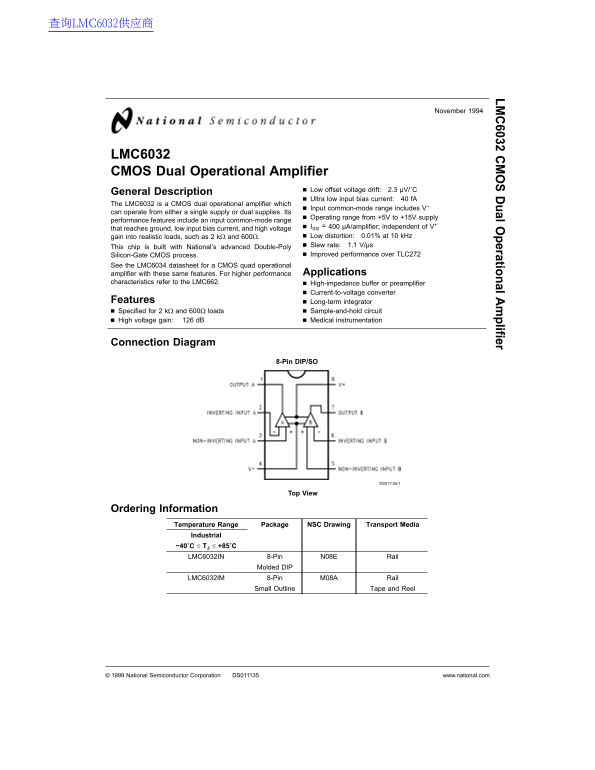
Connection Diagram
8-Pin DIP/SO
DS011135-1
Ordering Information
Temperature Range Package NSC Drawing Transport Media Industrial −40˚C TJ +85˚C LMC6032IN 8-Pin N08E Rail
Molded DIP
LMC6032IM 8-Pin M08A Rail
Small Outline Tape and Reel
National Semiconductor Corporation DS011135 www.national.com
Page Summary Contents For National Semiconductor LMC6032 CMOS Dual Operational Amplifier Data Sheet
Manual Details
| Brand | National |
|---|---|
| Pages | 13 |
| File Size | 294.04 KB |
| Published | June 18, 2026 |
Enter the captcha to get the download link:

Frequently Asked Questions
What is the operating voltage range for this amplifier?
It can operate from a +5V to +15V supply and supports both single or dual supplies.
What are the available package types and industrial temperature range?
Available packages include 8-Pin DIP/SO, rated for an industrial temperature range of -40°C to +85°C.
How is the differential input voltage specified for high CMRR?
For a Common Mode Rejection Ratio (CMRR) of ≥ 50 dB, the common mode voltage must be between minimum limits shown in the datasheet.
What is the maximum sourcing output current available at 15V supply?
The typical sourcing output current at V=15V peaks at 23 mA.