National Semiconductor LMC6082 Precision CMOS Dual Operational Amplifier Data Sheet
Summary
This high-precision dual operational amplifier provides exceptional performance with ultra-low offset voltage and minimal input bias current, making it ideal for sensitive analog designs. It supports single-supply operation (4.5V to 15V) while maintaining a rail-to-rail output swing and high gain. The included technical manual offers comprehensive guidelines on operating parameters, electrical characteristics, and required specifications. This device is essential for engineers designing critical precision circuits in demanding fields, including medical instrumentation, sample/hold circuits, and sensor signal processing.
Page 1 Text Content
查询LMC6082供应商
LM recision ual O perational A plifier
December
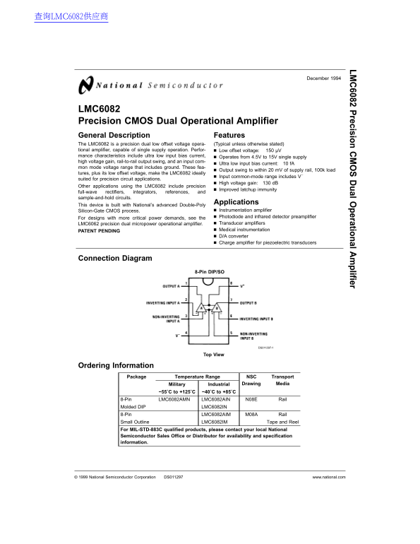
LMC6082 Precision CMOS Dual Operational Amplifier General Description Features The LMC6082 is precision dual low offset voltage opera- (Typical unless otherwise stated) tional amplifier, capable of single supply operation. Perfor- Low offset voltage: µV mance characteristics include ultra low input bias current, Operates from 4.5V to 15V single supply high voltage gain, rail-to-rail output swing, and an input com-
Ultra low input bias current: f A
mon mode voltage range that includes ground. These fea-
Output swing to within m V of supply rail, 100k load
tures, plus its low offset voltage, make the LMC6082 ideally
Input common-mode range includes V−
suited for precision circuit applications.
High voltage gain: d B
Other applications using the LMC6082 include precision
Improved latchup immunity
full-wave rectifiers, integrators, references, and sample-and-hold circuits.
Applications
This device is built with National’s advanced Double-Poly
Silicon-Gate CMOS process. Instrumentation amplifier For designs with more critical power demands, see the Photodiode and infrared detector preamplifier LMC6062 precision dual micropower operational amplifier. Transducer amplifiers PATENT PENDING Medical instrumentation D/A converter Charge amplifier for piezoelectric transducers
Connection Diagram
8-Pin DIP/SO
DS011297-1
Ordering Information
Package Temperature Range NSC Transport
Industrial Drawing Media Military
−55˚C to +125˚C −40˚C to +85˚C
8-Pin LMC6082AMN LMC6082AIN N08E Rail Molded DIP LMC6082IN 8-Pin LMC6082AIM M08A Rail Small Outline LMC6082IM Tape and Reel For MIL-STD-883C qualified products, please contact your local National Semiconductor Sales Office or Distributor for availability and specification information.
National Semiconductor Corporation DS011297 www.national.com
Page Summary Contents For National Semiconductor LMC6082 Precision CMOS Dual Operational Amplifier Data Sheet
Manual Details
| Brand | National |
|---|---|
| Pages | 12 |
| File Size | 325.01 KB |
| Published | June 18, 2026 |
Enter the captcha to get the download link:
