National Semiconductor LMC272 CMOS Dual Low Cost Rail to Rail Output Operational Amplifier Data Sheet
Summary
The LMC272 is a high-performance, low-cost CMOS dual operational amplifier featuring excellent rail-to-rail output swing and exceptional low voltage operation (down to 2.7V). This highly reliable component offers low power consumption and impressive isolation, making it ideal for complex analog designs. It is perfect for engineers developing portable instruments, photodetector preamplifiers, D/A converters, or those seeking cost-effective upgrades for existing electronic systems requiring high precision in small footprints.
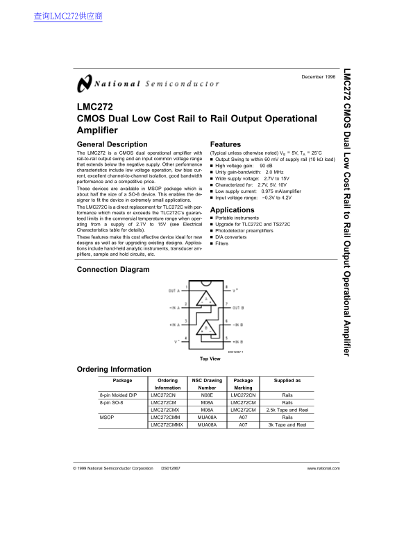
Page 1 Text Content
查询LMC272供应商
LM ual Low ost ailto ail O utput perational A plifier
December
LMC272 CMOS Dual Low Cost Rail to Rail Output Operational Amplifier General Description Features The LMC272 is CMOS dual operational amplifier with (Typical unless otherwise noted) VS 5V, TA 25˚C rail-to-rail output swing and an input common voltage range Output Swing to within m V of supply rail (10 kΩ load) that extends below the negative supply. Other performance High voltage gain: d B characteristics include low voltage operation, low bias cur-
Unity gain-bandwidth: 2.0 MHz
rent, excellent channel-to-channel isolation, good bandwidth
Wide supply voltage: 2.7V to 15V
performance and competitive price.
Characterized for: 2.7V, 5V, 10V
These devices are available in MSOP package which is
Low supply current: 0.975 m A/amplifier
about half the size of SO-8 device. This enables the de-
Input voltage range: −0.3V to 4.2V
signer to fit the device in extremely small applications. The LMC272C is direct replacement for TLC272C with per-
Applications
formance which meets or exceeds the TLC272C’s guaran-
teed limits in the commercial temperature range when oper- Portable instruments
ating from supply of 2.7V to 15V (see Electrical Upgrade for TLC272C and TS272C Characteristics table for details). Photodetector preamplifiers These features make this cost effective device ideal for new D/A converters designs as well as for upgrading existing designs. Applica- Filters tions include hand-held analytic instruments, transducer am- plifiers, sample and hold circuits, etc.
Connection Diagram
DS012867-1
Ordering Information
Package Ordering NSC Drawing Package Supplied as
Information Number Marking
8-pin Molded DIP LMC272CN N08E LMC272CN Rails 8-pin SO-8 LMC272CM M08A LMC272CM Rails
LMC272CMX M08A LMC272CM 2.5k Tape and Reel
MSOP LMC272CMM MUA08A A07 Rails
LMC272CMMX MUA08A A07 3k Tape and Reel
National Semiconductor Corporation DS012867 www.national.com
Page Summary Contents For National Semiconductor LMC272 CMOS Dual Low Cost Rail to Rail Output Operational Amplifier Data Sheet
Manual Details
| Brand | National |
|---|---|
| Pages | 16 |
| File Size | 462.06 KB |
| Published | June 17, 2026 |
Enter the captcha to get the download link:

Frequently Asked Questions
What is the operational voltage range for the LMC272?
The supply voltage supports a range of 2.5V to 15V.
Is this amplifier suitable for small applications?
Yes, it comes in an MSOP package and has low supply current (0.975 mA/amplifier), making it suitable for extremely small designs.
What is the high voltage gain of this operational amplifier?
The device boasts a high voltage gain of 90 dB.
Can the LMC272 perform in different environments?
It has an Operating Temperature Range of 0°C to +70°C (for the LMC272C).
How does the output swing compare to the supply rails?
The output can swing to within 60 mV of the supply rail, extending below the negative rail.