ST TDA7297 15+15W Dual Bridge Amplifier Data Sheet User Manual
Summary
The TDA7297 is a robust dual bridge amplifier specialized for integration into TV and portable radio applications. This technical manual provides comprehensive insights into the device's operation, detailing full electrical specifications, wide supply voltage range (6V–18V), and built-in protections including thermal overload and short circuit safeguards. It guides users through optimal implementation circuits—such as methods to prevent speaker "pop" and "click" noise during power cycles—making it an essential technical resource for embedded developers designing reliable, high-performance audio equipment.
Page 1 Text Content
TDA7297
15+15W DUAL BRIDGE AMPLIFIER
WIDE SUPPLY VOLTAGE RANGE (6V -18V)
TECHNOLOGY BI20II
MINIMUM EXTERNAL COMPONENTS – NO SVR CAPACITOR – NO BOOTSTRAP – NO BOUCHEROT CELLS – INTERNALLY FIXED GAIN STAND-BY & MUTE FUNCTIONS SHORT CIRCUIT PROTECTION THERMAL OVERLOAD PROTECTION
Multiwatt 15
DESCRIPTION ORDERING NUMBER: TDA7297
The TDA7297 is a dual bridge amplifier specially designed for TV and Portable Radio applications.
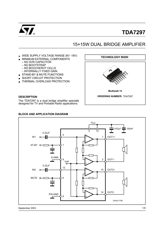
BLOCK AND APPLICATION DIAGRAM
IN1 OUT1+
ST-BY
S-GND
OUT1-
IN2 OUT2+
OUT2-
PW-GND
D94AU175B
September 2003 1/9
Page Summary Contents For ST TDA7297 15+15W Dual Bridge Amplifier Data Sheet User Manual
Manual Details
| Brand | Dual |
|---|---|
| Pages | 9 |
| File Size | 174.22 KB |
| Published | June 03, 2026 |
Enter the captcha to get the download link:

Frequently Asked Questions
Is the TDA7297 suitable for applications requiring complex microprocessor control?
Yes, microprocessor applications can use specific signaling sequences to manage St-by and mute signals effectively.