# A B C D E F G H I J K L M N O P Q R S T U V W X Y Z

ST L6206DMOS Dual Full Bridge Driver Data Sheet

Summary

The L6206 is a professional DMOS Dual Full Bridge power driver optimized for advanced motor control systems. This manual provides comprehensive technical specifications, including absolute maximum ratings and operational parameters across multiple packages (PowerDIP24, PowerSO36, SO24). It covers circuit operation, diagnostic outputs, critical safety features like overcurrent detection, and thermal protection shutdowns. Ideal for electrical engineers and designers requiring reliable, high-performance drivers for DC motor applications.
📄 Preview PAGE OF 23

Page 1 Text Content

DMOS DUAL FULL BRIDGE DRIVER

OPERATING SUPPLY VOLTAGE FROM 8 TO 52V 5.6A OUTPUT PEAK CURRENT (2.8A DC) RDS(ON) 0.3Ω TYP. VALUE @ Tj = 25 °C OPERATING FREQUENCY UP TO 100KHz PROGRAMMABLE HIGH SIDE OVERCURRENT

DETECTION AND PROTECTION Power DIP24 Power SO36

DIAGNOSTIC OUTPUT PARALLELED OPERATION

ORDERING NUMBERS:

CROSS CONDUCTION PROTECTION L6206N (Power DIP24)

THERMAL SHUTDOWN L6206PD (Power SO36) L6206D (SO24)

UNDER VOLTAGE LOCKOUT INTEGRATED FAST FREE WHEELING DIODES

BCD technology, which combines isolated DMOS

TYPICAL APPLICATIONS

Power Transistors with CMOS and bipolar circuits on

BIPOLAR STEPPER MOTOR

the same chip. Available in Power DIP24 (20+2+2),

DUAL OR QUAD DC MOTOR

Power SO36 and SO24 (20+2+2) packages, the L6206 features thermal shutdown and a non-dissipa-

DESCRIPTION tive overcurrent detection on the high side Power

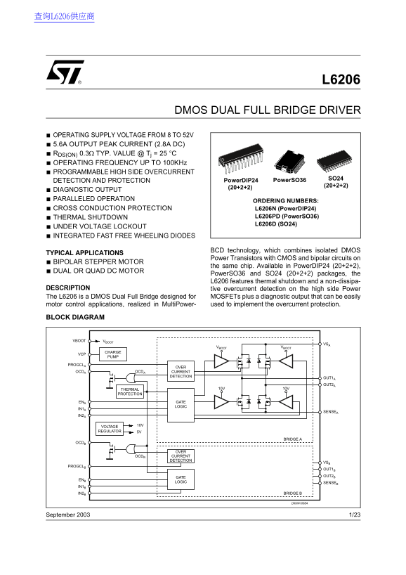
The L6206 is a DMOS Dual Full Bridge designed for MOSFETs plus a diagnostic output that can be easily motor control applications, realized in Multi Power- used to implement the overcurrent protection.

BLOCK DIAGRAM

VBOOT VBOOT

VBOOT VBOOT

CHARGE

PROGCLA

OCDA OCDA CURRENT

DETECTION

OUT1A OUT2A

THERMAL 10V 10V

PROTECTION

ENA GATE

LOGIC

SENSEA

VOLTAGE REGULATOR 5V

BRIDGE A

OVER OCDB CURRENT DETECTION

PROGCLB

OUT1B OUT2B

LOGIC SENSEB

IN1B IN2B BRIDGE B

D99IN1088A

September 2003 1/23

Page Summary Contents For ST L6206DMOS Dual Full Bridge Driver Data Sheet

Page 1 DMOS DUAL FULL BRIDGE DRIVER OPERATING SUPPLY VOLTAGE FROM 8 TO 52V 5.6A OUTPUT PEAK CURRENT (2.8A DC) RDS(ON) 0.3Ω TYP. VALUE @ Tj = 25 °C OPERATING FREQUENCY UP TO 100KHz PROGRAMMABLE HIGH SIDE OVER...
Page 2 ABSOLUTE MAXIMUM RATINGS Symbol Parameter Test conditions Value Unit VS Supply Voltage VSA = VSB = VS VOD Differential Voltage between VSA = VSB = VS = 60V; VSA, OUT1A, OUT2A, SENSEA and VSENSEA = VSE...
Page 3 THERMAL DATA Symbol Description Power DIP24 SO24 Power SO36 Unit Rth-j-pins Maximum Thermal Resistance Junction-Pins °C/W Rth-j-case Maximum Thermal Resistance Junction-Case °C/W Rth-j-amb1 °C/W Maxim...
Page 4 PIN DESCRIPTION PACKAGE Power SO36 Name Type Function SO24/ Power DIP24 PIN # PIN # IN1A Logic input Bridge A Logic Input 1. IN2A Logic input Bridge A Logic Input 2. SENSEA Power Supply Bridge A Sourc...
Page 5 PIN DESCRIPTION (continued) PACKAGE Power SO36 Name Type Function SO24/ Power DIP24 PIN # PIN # VCP Output Charge Pump Oscillator Output. ENA Logic Input Bridge A Enable. LOW logic level switches OFF ...
Page 6 ELECTRICAL CHARACTERISTICS (continued) (Tamb = 25 °C, Vs = 48V, unless otherwise specified) Symbol Parameter Test Conditions Min Typ Max Unit IIH High Level Logic Input Current 7V Logic Input Voltage ...
Page 7 Figure 1. Switching Characteristic Definition Vth(ON) Vth(OFF) 10% D01IN1316 t FALL t RISE t D(OFF)EN t D(ON)EN Figure 2. Overcurrent Detection Timing Definition OCD Threshold D01IN1222 t OCD(OFF)t OC...
Page 8 CIRCUIT DESCRIPTION these pins. Two configurations are shown in Fig. 5 and Fig. 6. If driven by an open drain (collector) struc- POWER STAGES and CHARGE PUMP ture, a pull-up resistor REN and a capacit...
Page 9 NON-DISSIPATIVE OVERCURRENT DETECTION AND PROTECTION In addition to the PWM current control, an overcurrent detection circuit (OCD) is integrated. This circuit can be used to provides protection again...
Page 10 Figure 7. Overcurrent Protection Simplified Schematic OUT1A OUT2A VSA POWER SENSE HIGH SIDE DMOSs OF 1 cell THE BRIDGE A POWER SENSE POWER DMOS 1 cell POWER DMOS µC or LOGIC TO GATE n cells n cells LO...
Page 11 Figure 9. Output Current Protection Threshold versus RCL Value [µ s] 4.5 IS I SOVER [A] R CL [ Ω Figure 10. t DISABLE versus CEN and REN (VDD = 5V).
Page 12 Figure 11. t DELAY versus CEN (VDD = 5V). td el ay s] Cen [n F] THERMAL PROTECTION In addition to the Ovecurrent Detection, the L6206 integrates a Thermal Protection for preventing the device destruct...
Page 13 APPLICATION INFORMATION A typical application using L6206 is shown in Fig. 12. Typical component values for the application are shown in Table 2. A high quality ceramic capacitor in the range of 100 t...
Page 14 PARALLELED OPERATION The outputs of the L6206 can be paralleled to increase the output current capability or reduce the power dissi- pation in the device at a given current level. It must be noted, ho...
Page 15 To operate the device in parallel and maintain a lower over current threshold, Half Bridge 1 and the Half Bridge 2 of the Bridge A can be connected in parallel and the same done for the Bridge B as sh...
Page 16 It is also possible to parallel the four Half Bridges to obtain a simple Half Bridge as shown in Fig. 15. In this configuration the, the over current threshold is equal to twice the minimum threshold ...
Page 17 OUTPUT CURRENT CAPABILITY AND IC POWER DISSIPATION In Fig. 16 and Fig. 17 are shown the approximate relation between the output current and the IC power dissipa- tion using PWM current control driving...
Page 18 Figure 18. Mounting the Power SO package. Slug soldered Slug soldered Slug soldered to PCB with to PCB with to PCB with dissipating area plus ground layer dissipating area dissipating area contacted t...
Page 19 Figure 22. Typical Quiescent Current vs. Figure 25. Typical High-Side RDS(ON) vs. Supply Voltage Supply Voltage Iq [m A] RDS(ON) [Ω] fsw = 1k Hz Tj = 25°C 0.380 0.376 Tj = 85°C Tj = 25°C Tj = 125°C VS...
Page 20 mm inch MIN. TYP. MAX. MIN. TYP. MAX. OUTLINE AND 3.60 0.141 MECHANICAL DATA 10°(max.) °(max.) Power SO36 (1): "D" and "E1" do not include mold flash or protrusions - Mold flash or...
Page 21 mm inch DIM. OUTLINE AND MIN. TYP. MAX. MIN. TYP. MAX. MECHANICAL DATA Powerdip 24 ̊min, 15 ̊max. SDIP24L
Page 22 mm inch DIM. OUTLINE AND MIN. TYP. MAX. MIN. TYP. MAX. MECHANICAL DATA Weight: 0.60gr 0˚ (min.), 8˚ (max.) ddd 0.10 0.004 (1) “D” dimension does not include mold flash, protusions or gate SO24 burrs. ...
Page 23 Information furnished is believed to be accurate and reliable. However, STMicroelectronics assumes no responsibility for the consequences of use of such information nor for any infringement of patents...

Manual Details

Brand Dual
Pages 23
File Size 402.58 KB
Published May 20, 2026
177 views

Enter the captcha to get the download link:

captcha

Frequently Asked Questions

What is the recommended operating temperature range?

The extended operating temperature range is -40 to 150 °C.

How can I check for overcurrent or thermal protection status on Bridge A or B?

Overcurrent detection/thermal protection uses an internal open drain transistor (OCD) which pulls to GND when triggered.

What does the L6206 feature regarding power rating and packages?

It is a DMOS Dual Full Bridge available in PowerDIP24, PowerSO36, or SO24 packages, featuring thermal shutdown and non-dissipative overcurrent detection.