Infineon TLE6282G Dual Half Bridge Driver IC Specifications
Summary
Optimize power control with this dual half-bridge driver IC, designed for advanced MOSFET power stages requiring robust management. This manual details comprehensive functionality, including adjustable dead time, short circuit detection, and undervoltage protection tailored for high reliability in extreme conditions. It is ideally suited for automotive systems, specifically motor bridges, injector, and valve applications powering 12V, 24V, and 48V networks.
Page 1 Text Content
Data Sheet TLE6282G
Dual Half Bridge Driver IC Features Product Summary • Compatible to very low ohmic normal
Turn on current IGxx(on) 850 m A
level input N-Channel MOSFETs
Turn off current IGxx(off) 580 m A
• Separate input for each MOSFET
Supply voltage range VVs 7.5 … 60 V
• PWM frequency up to 50 k Hz
Gate Voltage VGS 10 V
• Operates down to 7.5V
Temperature range TJ -40...+150 °C
supply voltage • Low EMC sensitivity and emission • Adjustable dead time with shoot through protection • Deactivation of dead time and shoot through protection possible • Short circuit protection for each Mosfet • Driver undervoltage shut down • Reverse polarity protection for the driver IC • Disable function • Input with TTL characteristics • 1 bit diagnosis • Integrated bootstrap diodes
P-DSO 20
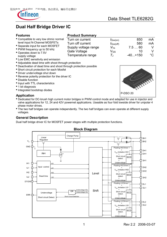
Application • Dedicated for DC-brush high current motor bridges in PWM control mode and adapted for use in injector and valve applications for 12, 24 and 42V powernet applications. Useable as four fold lowside driver for unipolar 4 phase motor drives. • The two half bridges can operate independently. The two half bridges can even operate at different supply voltages.
General Description Dual half bridge driver IC for MOSFET power stages with multiple protection functions.
Block Diagram Charge Pump
Linear
Regulator
VS BH2
Floating HS Driver 1
VGS limitation HS1
INH GH1
Short circuit
detect.
Undervoltage
IH1 HS1
Floating HS Driver 2
Input control DH2
IL1 LS1
VGS limitation HS2
IH2 HS2
Level Short circuit
Dead time detect.
IL2 LS2
Undervoltage
DT/DIS
Floating LS Driver 1
VGS limitation LS1 GL1
Undervoltage HSx
OR Shift
Undervoltage LSx Short circuit
Undervoltage SCD
detect.
Short Circuit Detection
Short circuit Detect.
Undervoltage
DL2Floating LS Driver 2 VGS limitation LS2 GL2
Short circuit
detect.
Undervoltage
1 Rev 2.2 2006-03-07
Page Summary Contents For Infineon TLE6282G Dual Half Bridge Driver IC Specifications
Manual Details
| Brand | Dual |
|---|---|
| Pages | 14 |
| File Size | 234.92 KB |
| Published | May 28, 2026 |
Enter the captcha to get the download link:

Frequently Asked Questions
What types of applications is the TLE6282G designed for?
It is primarily intended for DC-brush high current motor bridges, and it can also be used in injector and valve applications for various powernets (12, 24, or 42V).
How can I adjust or disable the dead time control?
The DT/DIS pin allows setting adjustable dead time using an external resistor, or enabling deactivation by connecting it to 0V.
What is the acceptable supply voltage range for this IC?
The general system supply voltage (Vs) operates within a range of 7.5 V to 60 V.
Is there a way to modify the Short Circuit Detection (SCD) sensitivity?
Yes, using voltage divider networks across the MOSFETs allows you to increase the SCD current limit threshold for both high and low side switches.