Fairchild Fan7080_GF085 Half Bridge Gate Driver Data Handbook
Summary
This high-voltage half-bridge gate driver IC is designed to provide stable and robust control for MOSFET or IGBT gates in demanding motor drive applications. Featuring adjustable dead time control, a reset input, and tolerance to negative transient voltages up to 600V, it ensures reliable operation even under extreme $\text{dv}/\text{dt}$ noise. The manual provides detailed technical specifications, including electrical characteristics and pin definitions necessary for integration into junction boxes and full/half-bridge circuits. It is the ideal solution for professional motor power systems requiring high switching performance and stability.
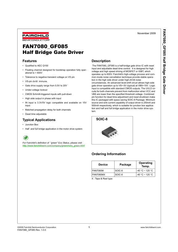
Page 1 Text Content
FA 7080_G F085 H alf B ridge G ate D river
November 2009
FAN7080_GF085 Half Bridge Gate Driver Features Description Qualified to AEC Q100 The FAN7080_GF085 is a half-bridge gate drive IC with reset
input and adjustable dead time control. It is designed for high
Floating channel designed for bootstrap operation fully oper-
voltage and high speed driving of MOSFET or IGBT, which
ational to + 600V
operates up to 600V. Fairchild's high-voltage process and com-
Tolerance to negative transient voltage on VS pin mon-mode noise cancellation technique provide stable opera-
tion in the high side driver under high-d V/dt noise
VS-pin dv/dt immune.
circumstances. An advanced level-shift circuit allows high-side
Gate drive supply range from 5.5V to 20V gate driver operation up to VS=-5V (typical) at VBS=15V. Logic
input is compatible with standard CMOS outputs. The UVLO cir-
Under-voltage lockout
cuits for both channels prevent from malfunction when VCC and
CMOS Schmitt-triggered inputs with pull-down VBS are lower than the specified threshold voltage. Combined
pin function for dead time adjustment and reset shutdown make
High side output in phase with input
this IC packaged with space saving SOIC-8 Package. Minimum
IN input is 3.3V/5V logic compatible and available on 15V source and sink current capability of output driver is 250m A and input 500m A respectively, which is suitable for junction box applica-
tion and half and full bridge application in the motor drive sys-
Matched propagation delay for both channels
Dead time adjustable
Typical Applications SOIC-8
Junction Box
Half and full bridge application in the motor drive system
For Fairchild’s definition of “green” Eco Status, please visit: http://www.fairchildsemi.com/company/green/rohs_green.html
Ordering Information
Operating
Device Package
Temp.
FAN7080M SOIC-8 -40 °C ~ 125 °C FAN7080MX SOIC-8 -40 °C ~ 125 °C X : Tape & Reel type
©2009 Fairchild Semiconductor Corporation www.fairchildsemi.com FAN7080_GF085 Rev. 1.0.0
Page Summary Contents For Fairchild Fan7080_GF085 Half Bridge Gate Driver Data Handbook
Manual Details
| Brand | Fairchild |
|---|---|
| Pages | 17 |
| File Size | 325.02 KB |
| Published | June 20, 2026 |
Enter the captcha to get the download link:

Frequently Asked Questions
What types of applications are suitable for the FAN7080_GF085?
It is well-suited for junction box, half, and full bridge applications in motor drive systems.
How does the device handle high-speed noise conditions?
It uses a mode noise cancellation technique and has VS-pin dv/dt immunity to provide stable operation under high-dV/dt noise.
Is the logic input compatible with standard CMOS outputs?
Yes, the logic input is compatible with standard CMOS outputs. The IN pin requires 3.3V/5V logic compatibility.
What are the recommended operating conditions for the device?
The unit should operate within an ambient temperature range of -40°C to 125°C, and the supply voltage (VCC) must be between 5.5V and 20V.