# A B C D E F G H I J K L M N O P Q R S T U V W X Y Z

Fairchild Fan73933 Half-Bridge Gate Drive IC Data Handbook

Summary

The FAN73933 is a robust half-bridge gate driver IC designed for high-speed power switching applications up to +600V. This manual details the device's advanced features, including programmable dead-time control and built-in noise cancellation, ensuring stable operation in harsh environments. It is essential reading for electrical engineers and designers of complex power electronics, such as motor drive inverters, DC-DC converters, and high-power bridge circuits.
📄 Preview PAGE OF 17

Page 1 Text Content

FA 73933 — alf-B ridge G ate D river

December 2009

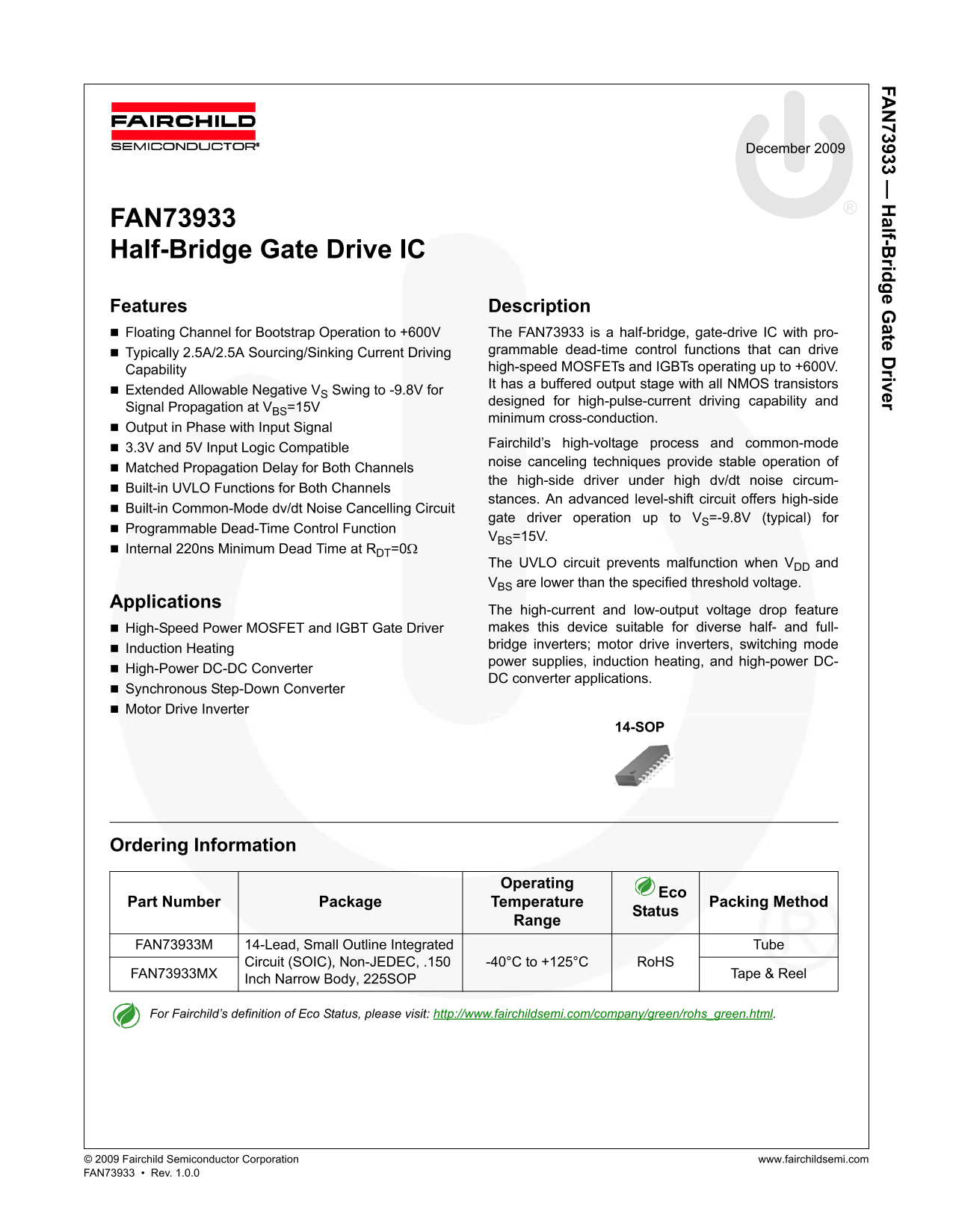
FAN73933 Half-Bridge Gate Drive IC

Features Description Floating Channel for Bootstrap Operation to +600V The FAN73933 is a half-bridge, gate-drive IC with pro-

Typically 2.5A/2.5A Sourcing/Sinking Current Driving grammable dead-time control functions that can drive Capability high-speed MOSFETs and IGBTs operating up to +600V. It has a buffered output stage with all NMOS transistors

Extended Allowable Negative VS Swing to -9.8V for

designed for high-pulse-current driving capability and

Signal Propagation at VBS=15V

minimum cross-conduction.

Output in Phase with Input Signal

Fairchild’s high-voltage process and common-mode

3.3V and 5V Input Logic Compatible

noise canceling techniques provide stable operation of

Matched Propagation Delay for Both Channels

the high-side driver under high dv/dt noise circum-

Built-in UVLO Functions for Both Channels

stances. An advanced level-shift circuit offers high-side

Built-in Common-Mode dv/dt Noise Cancelling Circuit

gate driver operation up to VS=-9.8V (typical) for

Programmable Dead-Time Control Function

VBS=15V.

Internal 220ns Minimum Dead Time at RDT=0Ω

The UVLO circuit prevents malfunction when VDD and VBS are lower than the specified threshold voltage.

Applications

The high-current and low-output voltage drop feature High-Speed Power MOSFET and IGBT Gate Driver makes this device suitable for diverse half- and full- bridge inverters; motor drive inverters, switching mode

Induction Heating

power supplies, induction heating, and high-power DC-

High-Power DC-DC Converter

DC converter applications.

Synchronous Step-Down Converter Motor Drive Inverter

14-SOP

Ordering Information

Operating

Part Number Package Temperature Packing Method

Status

Range

FAN73933M 14-Lead, Small Outline Integrated Tube

Circuit (SOIC), Non-JEDEC, .150 -40°C to +125°C Ro HS

FAN73933MX Tape & Reel

Inch Narrow Body, 225SOP

For Fairchild’s definition of Eco Status, please visit: http://www.fairchildsemi.com/company/green/rohs_green.html.

© 2009 Fairchild Semiconductor Corporation www.fairchildsemi.com FAN73933 • Rev. 1.0.0

Page Summary Contents For Fairchild Fan73933 Half-Bridge Gate Drive IC Data Handbook

Page 1 FA 73933 — alf-B ridge G ate D river December 2009 FAN73933 Half-Bridge Gate Drive IC Features Description Floating Channel for Bootstrap Operation to +600V The FAN73933 is a half-bridge, gate-drive I...
Page 2 FA 73933 — alf-B ridge G ate D river Typical Application Diagrams +15V Up to 600V RBOOT DBOOT IVERPU IVER FAN73933 Controller HIN NC LIN VB HOVSS R2 RDT CBOOT DT VS Load COM NC LO NC LSE EN ER TO VDD ...
Page 3 FA 73933 — alf-B ridge G ate D river Pin Configuration HIN NC LIN VB VSS HO DT VS COM NC LO NC VDD NC FA Figure 3. Pin Configurations (Top View) Pin Definitions Pin # Name Description HIN Logic Input ...
Page 4 FA 73933 — alf-B ridge G ate D river Absolute Maximum Ratings Stresses exceeding the absolute maximum ratings may damage the device. The device may not function or be opera- ble above the recommended ...
Page 5 FA 73933 — alf-B ridge G ate D river Electrical Characteristics VBIAS(VDD, VBS)=15.0V, VSS=COM=0V, DT=VSS and TA = 25°C, unless otherwise specified. The VIN and IIN parameters are referenced to VSS/CO...
Page 6 FA 73933 — alf-B ridge G ate D river Dynamic Electrical Characteristics VBIAS(VDD, VBS)=15.0V, VSS=COM=0V, CL=1000p F, DT=VSS and TA=25°C, unless otherwise specified. Symbol Parameter Conditions Min. ...
Page 7 FA 73933 — alf-B ridge G ate D river Typical Characteristics High-Side High-Side Low-Side Low-Side Temperature [°C] Temperature [°C] Figure 4. Turn-On Propagation Delay Figure 5. Turn-Off Propagation ...
Page 8 FA 73933 — alf-B ridge G ate D river Typical Characteristics (Continued) μA el ay at ch in [n s] [n s] DT1 DT2 (R =300KΩ) (RDT=300KΩ) DT Temperature [°C] Temperature [°C] Figure 10. Dead Time (RDT=300...
Page 9 FA 73933 — alf-B ridge G ate D river Typical Characteristics (Continued) [V μA SU V+ + [V PD Temperature [°C] Temperature [°C] Figure 16. Operating VCC Supply Current Figure 17. Operating VBS Supply C...
Page 10 FA 73933 — alf-B ridge G ate D river Typical Characteristics (Continued) μA [V [V IN + [ IH High-Side High-Side Low-Side Low-Side Temperature [°C] Temperature [°C] Figure 22. High-Level Output Voltage...
Page 11 FA 73933 — alf-B ridge G ate D river Typical Characteristics (Continued) High-Side High-Side Low-Side Low-Side Supply Voltage [V] Supply Voltage [V] Figure 28. Turn-On Propagation Delay Figure 29. Tur...
Page 12 FA 73933 — alf-B ridge G ate D river Typical Characteristics (Continued) High-Side High-Side Low-Side Low-Side Supply Voltage [V] Supply Voltage [V] Figure 34. High-Level Output Voltage Figure 35. Low...
Page 13 FA 73933 — alf-B ridge G ate D river Switching Time Definitions HIN HIN NC LIN LIN VB +15V HOVSS HO DT VS COM NC LO LO NC +15V VDD NC Figure 36. Switching Time Test Circuit FA HIN Shoot Though Prevent...
Page 14 FA 73933 — alf-B ridge G ate D river Application Information Negative VS Transient The bootstrap circuit has the advantage of being simple Figure 41. and Figure 42. show the commutation of the and low...
Page 15 FA 73933 — alf-B ridge G ate D river The FAN73933 has a negative VS transient performance Placement of Components curve, as shown in Figure 43. [V The recommended selection of component is as follows:...
Page 16 FA 73933 — alf-B ridge G ate D river Physical Dimensions PIN ONE INDICATOR TOP VIEW 0.20 LAND PATTERN RECOMMENDATION 1.80 MAX SEE DETAIL A 0.05MIN SIDE VIEW 0.10 MAX END VIEW GAGE NOTES: PLANE A) THIS...
Page 17 FA 73933 — alf-B ridge G ate D river © 2009 Fairchild Semiconductor Corporation www.fairchildsemi.com FAN73933 • Rev. 1.0.0 17

Manual Details

Brand Fairchild
Pages 17
File Size 1.92 MB
Published July 07, 2026
5 views

Enter the captcha to get the download link:

captcha

Frequently Asked Questions

How do I program the dead time?

Dead-time control can be managed externally using the dedicated DT pin and an external resistor.

What protective features prevent malfunctions during voltage drops?

The built-in UVLO (Under Voltage Latch-Up) circuit prevents malfunction when V/DD are lower than the specified threshold voltage.

Are there specific requirements for my PCB layout design?

Yes, regarding JESD51-2, the ground plane should not be placed under or near the high-voltage floating side.

What applications is this gate driver suitable for?

It is suitable for diverse half- and full-bridge inverters, motor drive inverters, and DC converters.