# A B C D E F G H I J K L M N O P Q R S T U V W X Y Z

ST TDA7266D Dual Bridge Amplifier Data Sheet

Summary

The TDA7266D is a powerful dual bridge amplifier delivering 5W+5W output across a wide supply voltage range (3.5–12V). Engineered with built-in features like short circuit and thermal protection, this compact module minimizes external components while offering crucial Stand-by and Mute functionality. Ideal for professional developers designing LCD TVs, PC motherboards, and premium portable audio devices, the manual provides detailed electrical specifications, mechanical dimensions, and expert application guides to ensure silent, robust integration into modern consumer electronics.
📄 Preview PAGE OF 13

Page 1 Text Content

TDA7266D

5W+5W DUAL BRIDGE AMPLIFIER

PRELIMINARY DATA

WIDE SUPPLY VOLTAGE RANGE (3.5 - 12V)

TECHNOLOGY BI20II

OUTPUT POWER 5+5W @THD = 10%, RL = 8Ω, VCC = 9.5V SINGLE SUPPLY MINIMUM EXTERNAL COMPONENTS NO SVR CAPACITOR NO BOOTSTRAP NO BOUCHEROT CELLS INTERNALLY FIXED GAIN

Power SO20 Slug Down STAND-BY & MUTE FUNCTIONS ORDERING NUMBER: TDA7266D

SHORT CIRCUIT PROTECTION THERMAL OVERLOAD PROTECTION

designed for LCD TV/Monitor, PC Motherboard, TV DESCRIPTION and Portable Audio applications.

The TDA7266D is a dual bridge amplifier specially

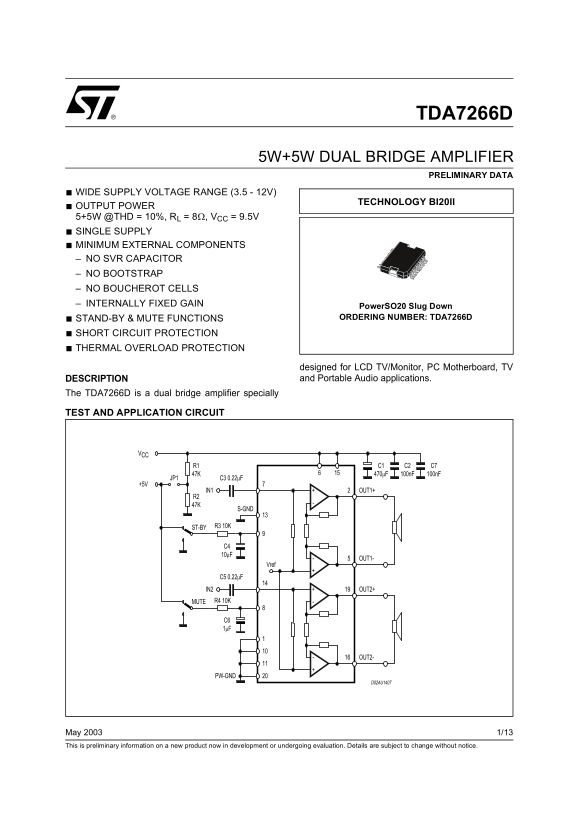
TEST AND APPLICATION CIRCUIT

JP1 C3 0.22µF

IN1 OUT1+ R2 47K

S-GND

ST-BY R3 10K

OUT1-

IN2 OUT2+

MUTE R4 10K

OUT2-

PW-GND

D02AU1407

May 2003 1/13 This is preliminary information on a new product now in development or undergoing evaluation. Details are subject to change without notice.

Page Summary Contents For ST TDA7266D Dual Bridge Amplifier Data Sheet

Page 1 TDA7266D 5W+5W DUAL BRIDGE AMPLIFIER PRELIMINARY DATA WIDE SUPPLY VOLTAGE RANGE (3.5 - 12V) TECHNOLOGY BI20II OUTPUT POWER 5+5W @THD = 10%, RL = 8Ω, VCC = 9.5V SINGLE SUPPLY MINIMUM EXTERNAL COMPONENT...
Page 2 TDA7266D ABSOLUTE MAXIMUM RATINGS Symbol Parameter Value Unit Vs Supply Voltage IO Output Peak Current (internally limited) 1.5 Ptot Total Power Dissipation (Tamb = 70°C Operating Temperature 0 to 70 ...
Page 3 TDA7266D ELECTRICAL CHARACTERISTCS (Refer to test circuit) VCC = 9.5V, RL = 8Ω, f = 1KHz, Tamb = 25°C unless otherwise specified) Symbol Parameter Test Condition Min. Typ. Max. Unit VCC Supply Range 3...
Page 4 TDA7266D APPLICATIVE SUGGESTIONS STAND-BY AND MUTE FUNCTIONS (A) Microprocessor Application In order to avoid annoying "Pop-Noise" during Turn-On/Off transients, it is necessary to guarantee...
Page 5 TDA7266D Figure 2. Microprocessor Driving Signals +VS(V) VIN (m V) VST-BY pin 9 1.8 VMUTE pin 8 Iq (m A) VOUT (V) PLAY MUTE ST-BY OFF ST-BY MUTE D02AU1411 B) Low Cost Application In low cost applicati...
Page 6 TDA7266D Figure 3. Stand-alone low-cost Application R1 OUT1+ 47K IN1 ST-BY S-GND OUT1- OUT2+ OUT2- PW-GND D02AU1410 PCB Layout and External Components: Regarding the PCB layout care must be taken for ...
Page 7 TDA7266D Dissipating Copper Area: Dissipated Power: The max dissipated power happens for a THD near 1% and is given by the formula: Pdmax Iq VCC+⋅= W( This gives for: Vcc = 9.5V, Rl = 8Ω ,Iq = 50m A a...
Page 8 TDA7266D Considering the dissipated power involved in the TDA7266D application that is in the range of 5W, as explained in a previous section, we suggest via holes ( see fig. 4). Using via holes a mor...
Page 9 TDA7266D Figure 6. Distortion vs Frequency Figure 9. Stand-By attenuation vs Vpin 9 THD(%) Attenuation (d B) Vcc = 9.5 V -20 Rl = 8 ohm -30 Pout = 100m W Pout = 2W frequency (Hz) Vpin.7 (V) Figure 7. ...
Page 10 TDA7266D Figure 12. THD+N vs Output Power Figure 13. THD+N vs Output Power THD(%) THD(%) Vcc=9.5V Rl=8ohm Vcc=12V f=1KHz Rl=16 ohm f = 1KHz Pout(W) Pout(W) Figure 14. PC Board Component Layout
Page 11 TDA7266D Figure 15. Evaluation Board Top Layer Layout Figure 16. Evaluation Board Bottom Layer Layout
Page 12 TDA7266D mm inch DIM. MIN. TYP. MAX. MIN. TYP. MAX. OUTLINE AND MECHANICAL DATA Weight: 1.9gr JEDEC MO-166 8˚ (typ.) 8˚ (max.) Power SO20 (1) “D and E1” do not include mold flash or protusions. - Mold...
Page 13 TDA7266D Information furnished is believed to be accurate and reliable. However, STMicroelectronics assumes no responsibility for the consequences of use of such information nor for any infringement o...

Manual Details

Brand Dual
Pages 13
File Size 196.64 KB
Published June 03, 2026
40 views

Enter the captcha to get the download link:

captcha

Frequently Asked Questions

How do I prevent 'Pop Noise' when turning the amplifier on?

Use external RC networks to slowly turn on biasing circuits, ensuring the Stand-by signal goes high first before charging input capacitors.

What is the typical output power and total distortion rate?

The typical measured output power is 4.3W for both channels, and the THD is specified as low as 0.2%.

What are the absolute maximum operational limits for this amplifier?

The maximum supply voltage (VCC) is 20V, and the total maximum power dissipation at 70°C ambient is 25W.

If using a microprocessor, what is the required signal sequence for activation?

Stand-by must go high first. Then, wait until input capacitors are charged before releasing the mute signal to avoid pop noise.