# A B C D E F G H I J K L M N O P Q R S T U V W X Y Z

ST LNBH26L Dual LNBS supply and control IC with step-up and I²C interface

Summary

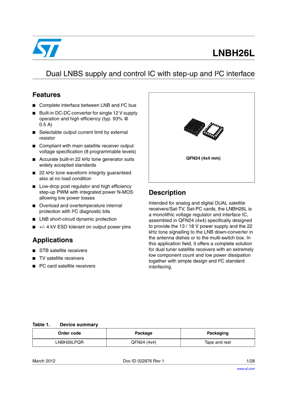
The LNBH26L is a high-efficiency interface IC designed as a complete solution for dual tuner satellite receivers. It manages the required power supply (13/18V) and 22 kHz signaling via an integrated, robust I²C bus connection. This technical guide provides comprehensive documentation covering device architecture, advanced diagnostic features, configurable output parameters, and detailed adherence to the full I²C communication protocol. It is essential for electronics engineers designing Set-Top Boxes (STBs), satellite TV receivers, or Sat-PC cards requiring reliable, low component count performance in professional analog and digital satellite applications.
📄 Preview 📖 Table of Contents Contents PAGE OF 28

Page 1 Text Content

LNBH26L

Dual LNBS supply and control IC with step-up and I²C interface

Features Complete interface between LNB and I²C bus Built-in DC-DC converter for single 12 V supply operation and high efficiency (typ. 93% @ 0.5 A) Selectable output current limit by external resistor Compliant with main satellite receiver output voltage specification (8 programmable levels)

QFN24 (4x4 mm)

Accurate built-in 22 k Hz tone generator suits widely accepted standards 22 k Hz tone waveform integrity guaranteed also at no load condition Low-drop post regulator and high efficiency step-up PWM with integrated power N-MOS Description allowing low power losses

Intended for analog and digital DUAL satellite

Overload and overtemperature internal

receivers/Sat-TV, Sat-PC cards, the LNBH26L is

protection with I²C diagnostic bits

a monolithic voltage regulator and interface IC,

LNB short-circuit dynamic protection

assembled in QFN24 (4x4) specifically designed +/- 4 k V ESD tolerant on output power pins to provide the 13 / 18 V power supply and the 22 k Hz tone signalling to the LNB down-converter in the antenna dishes or to the multi-switch box. In

Applications

this application field, it offers a complete solution for dual tuner satellite receivers with an extremely

STB satellite receivers

low component count and low power dissipation

TV satellite receivers

together with simple design and I²C standard

PC card satellite receivers interfacing.

Table 1. Device summary

Order code Package Packaging

LNBH26LPQR QFN24 (4x4) Tape and reel

March 2012 Doc ID 022876 Rev 1 1/28

www.st.com

Page Summary Contents For ST LNBH26L Dual LNBS supply and control IC with step-up and I²C interface

Page 1 LNBH26L Dual LNBS supply and control IC with step-up and I²C interface Features Complete interface between LNB and I²C bus Built-in DC-DC converter for single 12 V supply operation and high efficiency...
Page 2 Contents LNBH26L Contents Block diagram . . . . . . . . . . . . . . . . . . . . . . . . . . . . . . . . . . . . . . . . . . . . . . 3 Application information (valid for each section A/B) . . . . . . ....
Page 3 LNBH26L Contents 7.4 Status registers . . . . . . . . . . . . . . . . . . . . . . . . . . . . . . . . . . . . . . . . . . . . 19 Electrical characteristics . . . . . . . . . . . . . . . . . . . . . . ...
Page 4 Block diagram LNBH26L 1 Block diagram Figure 1. Block diagram Is en se DSQIN-A ADDR SDASCL DSQIN-B LX-A LX-B at ct rl PW TR I²C Digital core DAC Drop control PGND PGND Tone ctrl Diagnostics VUP-A Prot...
Page 5 LNBH26L Application information (valid for each section A/B) 2 Application information (valid for each section A/B) This IC has a built-in DC-DC step-up converter that, from a single source (8 V to 16...
Page 6 Application information (valid for each section A/B) LNBH26L 2.3 Data encoding by external Di SEq C envelope control through the DSQIN pin If an external Di SEq C envelope source is available, it is p...
Page 7 LNBH26L Application information (valid for each section A/B) 2.6 Diagnostic and protection functions The LNBH26L has 4 diagnostic internal functions provided via the I²C bus, by reading 4 bits on the ...
Page 8 Application information (valid for each section A/B) LNBH26L 2.9 PNG: input voltage minimum detection When input voltage (VCC pin) is lower than LPD (low power diagnostic) minimum thresholds, the PNG ...
Page 9 LNBH26L Pin configuration 3 Pin configuration Figure 5. Pin connections (top view) GNDDSQIN-B DSQIN-A VUP-A VOUT-A GND GND GND GND VCC LX- BYP PGND GND LX- NC ADDR GND SCL SDA ISEL VOUT-B GNDVUP-B AM1...
Page 10 Pin configuration LNBH26L Table 2. Pin description (continued) Pin n° Symbol Name Pin function Input of channel B linear post-regulator. The voltage on this pin Channel B VUP-B is monitored by the int...
Page 11 LNBH26L Maximum ratings 4 Maximum ratings Table 3. Absolute maximum ratings Symbol Parameter Value Unit VCC DC power supply input voltage pins -0.3 to 20 VUP DC input voltage -0.3 to 40 IOUT Output cu...
Page 12 Typical application circuits LNBH26L 5 Typical application circuits Figure 6. Di SEq C 1.x application circuit LNBOUT-A VUP-A VOUT-A C2-A C3-A LNBH26LD1-A C5-A D3-A R1 (RSEL) Di SEq C Byp DSQIN-A 22KH...
Page 13 LNBH26L I²C bus interface 6 I²C bus interface Data transmission from the main microprocessor to the LNBH26L, and vice versa, takes place through the 2-wire I²C bus interface, consisting of the 2-line ...
Page 14 I²C bus interface LNBH26L Figure 7. Data validity on the I²C bus Figure 8. Timing diagram of I²C bus Figure 9. Acknowledge on the I²C bus 14/28 Doc ID 022876 Rev 1
Page 15 LNBH26L I²C interface protocol 7 I²C interface protocol /A /A 7.1 Write mode transmission /A LR /A The LNBH26L interface protocol is made up of: a START condition (S) TH ER a chip address byte with th...
Page 16 I²C interface protocol LNBH26L 7.2 Read mode transmission In read mode the bytes sequence must be as follows: /A /A a START condition (S) a chip address byte with the LSb bit R/W=0 LR /A the register ...
Page 17 LNBH26L I²C interface protocol 7.3 Data registers The DATA 1..4 registers can be addressed both in write and read mode. In read mode they return the last writing byte status received in the previous w...
Page 18 I²C interface protocol LNBH26L Table 8. DATA 3 (read/write register. Register address = 0X4) Bit Name CH Value Description Bit 0 N/A Reserved. Keep to “0” (LSb) Bit 1 N/A Reserved. Keep to “0” Bit 2 P...
Page 19 LNBH26L I²C interface protocol 7.4 Status registers The STATUS 1, 2 registers can be addressed only in read mode and provide the diagnostic functions described in the following tables. Table 10. STATU...
Page 20 Electrical characteristics LNBH26L 8 Electrical characteristics Refer to Section 5, TJ from 0 to 85 °C, all DATA 1..4 register bits set to 0 unless VSEL1 = 1, RSEL = 11 kΩ, DSQIN = LOW, VIN = 12 V, IO...
Page 21 LNBH26L Electrical characteristics Table 12. Electrical characteristics of section A/B (continued) Symbol Parameter Test conditions Min. Typ. Max. Unit VLP threshold rising 7.2 Low power diagnostic (L...
Page 22 Electrical characteristics LNBH26L Table 13. Output voltage selection table (Data1 register, write mode) (1) VOUT -A/B VSEL4- VSEL3- VSEL2- VSEL1- VOUT VOUT pin Function A/B A/B A/B A/B min. max. volt...
Page 23 LNBH26L Package mechanical data 9 Package mechanical data In order to meet environmental requirements, ST offers these devices in different grades of ECOPACK® packages, depending on their level of env...
Page 24 Package mechanical data LNBH26L Figure 12. QFN24L (4x4 mm) package dimensions 24/28 Doc ID 022876 Rev 1
Page 25 LNBH26L Package mechanical data Tape & reel QFNxx/DFNxx (4x4) mechanical data mm. inch. Min. Typ. Max. Min. Typ. Max. Ao 4.35 0.171 Bo 4.35 0.171 Ko 1.1 0.043 Po 0.157 Doc ID 022876 Rev 1 25/28
Page 26 Package mechanical data LNBH26L Figure 13. QFN24L (4x4) footprint recommended data (mm) 26/28 Doc ID 022876 Rev 1
Page 27 LNBH26L Revision history 10 Revision history Table 17. Document revision history Date Revision Changes 01-Mar-2012 Initial release. Doc ID 022876 Rev 1 27/28
Page 28 LNBH26L Please Read Carefully: Information in this document is provided solely in connection with ST products. STMicroelectronics NV and its subsidiaries (“ST”) reserve the right to make changes, corr...

Manual Details

Brand Dual
Pages 28
File Size 938.64 KB
Published May 20, 2026
173 views

Enter the captcha to get the download link:

captcha

Frequently Asked Questions

How is the data encoding handled for this device?

Data can be encoded either by external DiSEqC envelope control via the DSQIN pin or using an external 22 kHz tone TTL signal.

What are the primary protection features available on the LNBH26L?

It provides internal protection for overload, overtemperature, and short-circuit conditions, along with +/- 4 kV ESD tolerance on output power pins.

Does the device offer flexible power operation?

Yes, it includes a built-in DC-DC converter supporting single 12 V supply and features up to 8 programmable voltage levels.

How can the user adjust the current output?

The output current limit is customizable and can be selected using an external resistor.