# A B C D E F G H I J K L M N O P Q R S T U V W X Y Z

ST ST6G3238BE Dual Supply Level Translator for SD/MiniSD/T-Flash with ±8kV Contact Discharge ESD Protection

Summary

The ST6G3238BE is a robust dual-supply low voltage CMOS Level Translator specifically designed for interfacing SD, MiniSD, and T-Flash memory modules. This IC efficiently translates voltage levels between mixed bus systems (e.g., 3.3V to 1.8V or 2.5V), simplifying complex hardware integration. It features high-speed operation, low power dissipation, and industry-leading ESD protection (up to ±15kV) for reliable data transmission in demanding environments. Ideal for embedded systems requiring stable, protected memory interfacing.
📄 Preview 📖 Table of Contents Contents PAGE OF 17

Page 1 Text Content

ST6G3238BE

Dual supply level translator for SD/ MINISD/ T-FLASH With ±8KV contact discharge ESD protection

Features High speed: t PD = 4.4ns (Typ.) at TA = 85°C VCCB = 2.7V VCCA = 1.8V Low power dissipation: ICCA = ICCB = 5µA (Max.) at TA = 85°C Balanced propagation delays: TPLH ≈ TPHL Power down protection on inputs and outputs

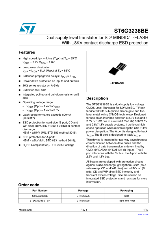
µTFBGA25

26Ω series resistor on A-Side EMI filter on B side Integrated pull-up and pull-down resistor on B side Description Operating voltage range:

The ST6G3238BE is a dual supply low voltage

VCCA (Opr) = 1.4V to VCCB

CMOS Level Translator for SD/ Mini SD/ T-Flash

VCCB (Opr) = 1.4V to 3.6V

fabricated with sub-micron silicon gate and five- Latch-up performance exceeds 500m A layer metal wiring C2MOS technology. Designed (JESD17) for use as an interface between a 3.3V bus and a 2.5V or 1.8V bus in a mixed 3.3V/1.8V, 3.3V/2.5V

ESD protection for card side (B port, CD and

and 2.5V/1.8V supply systems, it achieves high

WP pins) ±8k V, IEC 61000-4-2 ESD or contact

speed operation while maintaining the CMOS low

discharge:

power dissipation. The A port is designed to track

HBM > ±15k V (MIL STD 883 method 3015);

VCCA. The B port is designed to track VCCB.

ESD protection for A-port:

This device is intended for two-way asynchronous

HBM > ±2k V (MIL STD 883 method 3015);

communication between data buses and the

ROHS Compliant for µTFBGA25 Package

direction of data transmission is determined by CMD-dir/ DATA0-dir/ DAT123-dir inputs. The B- port interfaces with the 3V bus, the A-port with the 2.5V and 1.8V bus. All inputs are equipped with protection circuits against static discharge, giving them ±2k V (on A- side except CD and WP pins) and ±15k V on (B side, CD and WP pins) ESD immunity and transient excess voltage. See the section on integrated ESD protections and resistors for more information.

Order code Part Number Package Packaging

ST6 G3238BE µTFBGA25 Tube ST6G 3238BETBR µTFBGA25 Tape and Reel

March 2007 Rev 1 1/17

17www.st.com

Page Summary Contents For ST ST6G3238BE Dual Supply Level Translator for SD/MiniSD/T-Flash with ±8kV Contact Discharge ESD Protection

Page 1 ST6G3238BE Dual supply level translator for SD/ MINISD/ T-FLASH With ±8KV contact discharge ESD protection Features High speed: t PD = 4.4ns (Typ.) at TA = 85°C VCCB = 2.7V VCCA = 1.8V Low power dissi...
Page 2 Contents ST6G3238BE Contents Logic diagram . . . . . . . . . . . . . . . . . . . . . . . . . . . . . . . . . . . . . . . . . . . . . . . . 3 Pin connection and function . . . . . . . . . . . . . . . ....
Page 3 ST6G3238BE Logic diagram 1 Logic diagram Figure 1. Block diagram A-SIDE B-SIDE CMD-dir CMD.h CMD DATA0-dir DAT0.h DAT0 DAT123-dir DAT1.h DAT1 DAT2.h DAT2 DAT3.h DAT3 CLK.h R1 CLK-f R13 R14VCCA WP CD T...
Page 4 Pin connection and function ST6G3238BE 2 Pin connection and function Figure 2. Pin connection (top through view for µTFBGA) 1 2 3 4 5 DAT0-dir CMD-dir CMD.h DAT0.h DAT1.h DAT2.h DAT3.h µTFBGA25 CLK-f ...
Page 5 ST6G3238BE Pin connection and function 2.1 Pin function CMD, Command is a bi-directional line. The host and card drivers are operating in push- pull. DAT0-3, Data lines are bi-directional lines. The h...
Page 6 Summary description ST6G3238BE 3 Summary description Table 4. Truth table Function Output DAT1.h DAT1 CMD-dir DAT0-dir DAT123-dir CMD.h CMD DAT0.h DAT0 DAT2.h DAT2 DAT3.h DAT3 INPUT OUTPUT B = A OUTPU...
Page 7 ST6G3238BE Maximum rating 4 Maximum rating Stressing the device above the rating listed in the “Absolute Maximum Ratings” table may cause permanent damage to the device. These are stress ratings only ...
Page 8 DC and AC parameters ST6G3238BE 5 DC and AC parameters Table 7. DC specification Test conditions Value Symbol Parameter TA = 25°C -40 to 85°C Unit VCCA VCCB (V) (V) Min. Max. Min. Max. 1.4-1.95 0.65VC...
Page 9 ST6G3238BE DC and AC parameters Table 7. DC specification (continued) Test conditions Value Symbol Parameter TA = 25°C -40 to 85°C Unit VCCA VCCB (V) (V) Min. Max. Min. Max. 1.4-3.6 1.4-3.6 IOL = 100µ...
Page 10 DC and AC parameters ST6G3238BE Table 8. AC electrical characteristics (f = 1MHz, 50% duty cycle, CL = 30p F, RL = 500Ω) Test condition TA = -40 to 85 °C VCCA = 1.8 ± VCCA=1.8 ± 0.15V VCCA=2.5 ± 0.2V ...
Page 11 ST6G3238BE I/O and test circuit 6 I/O and test circuit Figure 3. Input and output equivalent circuit Figure 4. Test cicuit Table 11. Test values Test Switch t PLH, t PHL Open t PZL, t PLZ (VCC = 3.0 t...
Page 12 Waveforms ST6G3238BE 7 Waveforms Figure 5. Waveform - propagation delay (f = 1 MHz, 50% duty cycle) Table 12. Waveform symbol value Symbol 3.0 to 3.6V 2.3 to 2.7V 1.65 to 1.95V VIH VCC VCC VCC VM 1.5V...
Page 13 ST6G3238BE Package mechanical data 8 Package mechanical data In order to meet environmental requirements, ST offers these devices in ECOPACK® packages. These packages have a Lead-free second level int...
Page 14 Package mechanical data ST6G3238BE Table 13. µTFBGA25 mechanical data Dimension (mm) Dimension (inch) Dim Ref Min. Typ. Max Min. Typ. Max SE 0.25 0.010 Figure 6. Package dimensions
Page 15 ST6G3238BE Package mechanical data Table 14. µTFBGA25 tape and reel information Dimension (mm) Dimension (inch) Dim Ref Min. Typ. Max Min. Typ. Max A 330 12.992 C 12.8 13.2 0.504 0.519 D 20.2 0.795 N ...
Page 16 Revision history ST6G3238BE 9 Revision history Table 15. Revision history Date Revision Change 22-Mar-2007 First release
Page 17 ST6G3238BE Please Read Carefully: Information in this document is provided solely in connection with ST products. STMicroelectronics NV and its subsidiaries (“ST”) reserve the right to make changes, c...

Manual Details

Brand Dual
Pages 17
File Size 297.14 KB
Published May 20, 2026
153 views

Enter the captcha to get the download link:

captcha

Frequently Asked Questions

What voltage buses does this level translator support?

It is designed to interface between a 3.3V bus (B port) and either a 2.5V or 1.8V bus (A port).

How robust is the ESD protection on the different data ports?

The B-port can track >±15kV, while the A-port has protection up to ±2kV for most non-CD/WP pins.

What determines the direction of data transmission?

Data transfer direction is specifically determined by the CMD-dir, DATA0-dir, and DAT123-dir inputs.

What is the low power dissipation rating at 85°C?

The maximum current draw (I) during operation is limited to 5µA at T = 85°C.