# A B C D E F G H I J K L M N O P Q R S T U V W X Y Z

ST ST2329 2-bit dual supply level translator without direction control pin

Summary

Streamline complex data communications with the ST2329, a 2-bit dual supply level translator designed for multi-voltage systems. Enabling seamless, bidirectional signal transfer between components operating at differing voltage levels (V_L and V_CC), this device manages low power consumption while ensuring compatibility across wide operational ranges. Ideal for embedded systems, mobile devices, and ASIC/PLD integration, the ST2329 simplifies level shifting without directional control pins. Included documentation provides comprehensive specifications, detailed wiring diagrams, electrical characteristics, and application notes necessary for reliable design implementation.
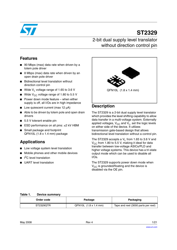
📄 Preview 📖 Table of Contents Contents PAGE OF 21

Page 1 Text Content

ST2329

2-bit dual supply level translator without direction control pin

Features 90 Mbps (max) data rate when driven by a totem pole driver 8 Mbps (max) data rate when driven by an open drain pole driver Bidirectional level translation without direction control pin Wide VL voltage range of 1.65 to 3.6 QFN10L (1.8 x 1.4 mm) Wide VCC voltage range of 1.80 to 5.5 Power down mode feature – when either supply is off, all I/Os are in high impedance

Description

Low quiescent current (max 12 µA) Able to be driven by totem pole and open drain The ST2329 is a 2-bit dual supply level translator drivers which provides the level shifting capability to allow

data transfer in a multi-voltage system. Externally

5.5 V tolerant enable pin

applied voltages, VCC and VL, set the logic levels

ESD performance on all pins: ±2 k V HBM

on either side of the device. It utilizes

Small package and footprint transmission gate-based design that allows QFN10L (1.8 1.4 mm) package bidirectional level translation without a control pin.

The ST2329 accepts a VL from 1.65 to 3.6 V and

Applications VCC from 1.80 to 5.5 V, making it ideal for data

transfer between low-voltage ASICs/PLD and

Low voltage system level translation

higher voltage systems. This device has a tri-state

Mobile phones and other mobile devices output mode which can be used to disable all

I/Os.

I2C level translation

UART level translation The ST2329 supports power down mode when VCC is grounded/floating and the device is disabled via the OE pin.

Table 1. Device summary

Order code Package Packaging

ST2329QTR QFN10L (1.8 x 1.4 mm) Tape and reel (3000 parts per reel)

May 2008 Rev 4 1/21

www.st.com

Page Summary Contents For ST ST2329 2-bit dual supply level translator without direction control pin

Page 1 ST2329 2-bit dual supply level translator without direction control pin Features 90 Mbps (max) data rate when driven by a totem pole driver 8 Mbps (max) data rate when driven by an open drain pole dri...
Page 2 Contents ST2329 Contents Pin settings . . . . . . . . . . . . . . . . . . . . . . . . . . . . . . . . . . . . . . . . . . . . . . . . 3 1.1 Pin connection . . . . . . . . . . . . . . . . . . . . . . ....
Page 3 ST2329 Pin settings 1 Pin settings 1.1 Pin connection Figure 1. Pin connection (top through view) I/OVCC1 I/OVL1 I/OVL2 I/OVCC2 NC NC CS00011 1.2 Pin description Table 2. Pin description Pin number Sy...
Page 4 Device block diagrams ST2329 2 Device block diagrams Figure 2. ST2329 block diagram VL ST2329 VL VCC I/O VL I/O GND GND = one-shot circuit * ST2329 has 2 channels. For simplicity, the above diagram sh...
Page 5 ST2329 Supplementary notes 3 Supplementary notes 3.1 Driver requirement The ST2329 may be driven by an open drain or totem pole driver and the nature of the device’s output is “open drain”. It must no...
Page 6 Maximum rating ST2329 4 Maximum rating Stressing the device above the rating listed in the “Absolute maximum ratings” table may cause permanent damage to the device. These are stress ratings only, and...
Page 7 ST2329 Electrical characteristics 5 Electrical characteristics Table 6. DC characteristics (over recommended operating conditions unless otherwise noted. All typical values are at TA = 25 o C) Test co...
Page 8 Electrical characteristics ST2329 Table 6. DC characteristics (over recommended operating conditions unless otherwise noted. All typical values are at TA = 25 o C) (continued) Test conditions Value Sy...
Page 9 ST2329 Electrical characteristics 5.1 AC characteristics (device driven by open drain driver) Table 7. AC characteristics - test conditions: VL = 1.65 −1.8 V (load CL p F; Rup 4.7 kΩ; driver tr tf ≤ 2...
Page 10 Electrical characteristics ST2329 Table 8. AC characteristics - test conditions: VL 2.5 −2.7 V (load CL p F; Rup 4.7 kΩ; driver tr tf ≤ 2 ns) over temperature range -40 °C to 85 °C VCC 2.7 −3.6 VCC 4....
Page 11 ST2329 Electrical characteristics 5.2 AC characteristics (device driven by totem pole driver ) Table 10. AC characteristics (test conditions: VL 1.65 −1.8 V (load CL p F; Rup kΩ; driver tr=tf ≤ 2 ns) ...
Page 12 Electrical characteristics ST2329 Table 11. AC characteristics (test conditions: VL 2.5 −2.7 V (load CL p F; Rup kΩ; driver tr tf ≤ 2 ns) over temperature range -40 °C to 85 °C) (continued) VCC 2.7 −3...
Page 13 ST2329 Electrical characteristics Figure 4. Test circuit VL VCC VL VCC 10 kΩ 10 kΩ VL VCC OPEN Pulse D.U.T generator CS14021 Table 13. Test circuit switches Switch Driving I/OVL Driving I/OVCC Open dr...
Page 14 Waveforms ST2329 6 Waveforms Table 14. Waveform symbol value Driving I/OVL Driving I/OVCC Symbol 1.8 ≤ VL ≤ VCC ≤ 3.3 ≤ VL ≤ VCC ≤ 1.8 ≤ VL ≤ VCC 3.3V ≤ VL ≤ VCC 2.5 5.0 2.5 5.0 VIH VL VL VCC VCC VIM ...
Page 15 ST2329 Waveforms Figure 6. Waveform - output enable and disable time (f MHz; 50% duty cycle)
Page 16 Package mechanical data ST2329 7 Package mechanical data In order to meet environmental requirements, ST offers these devices in ECOPACK® packages. These packages have a Lead-free second level interco...
Page 17 ST2329 Package mechanical data Table 15. QFN10L (1.8 1.4 mm) mechanical data Millimeters Symbol Typ Min Max Figure 8. QFN10L (1.8 1.4 mm) footprint recommendation
Page 18 Package mechanical data ST2329 Figure 9. QFN10L (1.8 1.4 mm) carrier tape Figure 10. QFN10L (1.8 1.4 mm) reel information - back view
Page 19 ST2329 Package mechanical data Figure 11. QFN10L (1.8 1.4 mm) reel information - front side
Page 20 Revision history ST2329 8 Revision history Table 16. Document revision history Date Revision Changes 15-May-2007 Initial release Modified title, added pin description and complete electrical 01-Oct-20...
Page 21 ST2329 Please Read Carefully: Information in this document is provided solely in connection with ST products. STMicroelectronics NV and its subsidiaries (“ST”) reserve the right to make changes, corre...

Manual Details

Brand Dual
Pages 21
File Size 428.40 KB
Published May 20, 2026
168 views

Enter the captcha to get the download link:

captcha

Frequently Asked Questions

What are the operating voltage ranges for the two supply sides?

The device supports V from 1.65 to 3.6 V and L from 1.80 to 5.5 V.

How is the level translation controlled or disabled?

It can be disabled via the OE pin, putting all I/Os into a high-impedance mode when low.

What is the maximum data rate supported under different driver types?

The max data rate is 90 Mbps (with totem pole) or 8 Mbps (with open drain).

Does it have power saving features?

Yes, it has a power down mode feature where all I/Os enter high impedance if either supply is off.