ST DCPL-WB-00D3 Wide-band, Dual-Path Directional Coupler with ISO Port User Manual and Data Sheet
Summary
This wide-band, dual-path directional coupler is engineered for accurately measuring cell phone transmission output power across multi-band telecommunication systems, such as GSM and WCDMA bands (824 MHz - 2170 MHz). Featuring ultra-low insertion loss and high directivity in both low and high paths, this component ensures reliable RF measurement. The accompanying manual provides comprehensive technical documentation, covering detailed electrical characteristics, full ESD rating compliance, and thorough RF performance data for professional use by telecom equipment developers.
Page 1 Text Content
DCPL-WB-00D3
Wide-band, dual-path directional coupler with ISO port
Features 50 Ω nominal input / output impedance Wide operating frequency range: 824 MHz-2170 MHz Low insertion loss (< 0.2 d B)
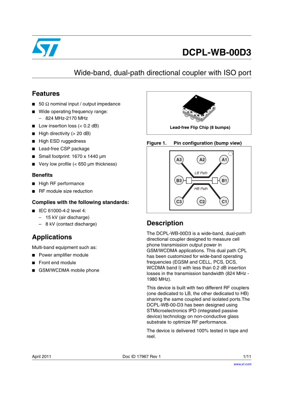
Lead-free Flip Chip (8 bumps)
High directivity (> 20 d B) High ESD ruggedness
Figure 1. Pin configuration (bump view)
Lead-free CSP package Small footprint: 1670 x 1440 µm
Very low profile (< 650 µm thickness)
LB Path
Benefits
High RF performance
HB Path
RF module size reduction
Complies with the following standards: C1C2C3
IEC 61000-4-2 level 4: 15 k V (air discharge)
8 k V (contact discharge) Description The DCPL-WB-00D3 is a wide-band, dual-path
Applications
directional coupler designed to measure cell phone transmission output power in
Multi-band equipment such as:
GSM/WCDMA applications. This dual path CPL
Power amplifier module
has been customized for wide-band operating Front end module frequencies (EGSM and CELL, PCS, DCS, WCDMA band I) with less than 0.2 d B insertion
GSM/WCDMA mobile phone
losses in the transmission bandwidth (824 MHz - 1980 MHz). This device is built with two different RF couplers (one dedicated to LB, the other dedicated to HB) sharing the same coupled and isolated ports.The DCPL-WB-00-D3 has been designed using STMicroelectronics IPD (integrated passive device) technology on non-conductive glass substrate to optimize RF performance. The device is delivered 100% tested in tape and reel.
April 2011 Doc ID 17967 Rev 1 1/11
www.st.com
Page Summary Contents For ST DCPL-WB-00D3 Wide-band, Dual-Path Directional Coupler with ISO Port User Manual and Data Sheet
Manual Details
| Brand | Dual |
|---|---|
| Pages | 11 |
| File Size | 138.45 KB |
| Published | June 01, 2026 |
Enter the captcha to get the download link:

Frequently Asked Questions
What is the nominal impedance for both RF paths?
The nominal input, output, coupled port, and isolated port impedances are all 50 Ω.
What standards does this coupler meet regarding ESD protection?
It complies with IEC 61000-4-2 level 4 for air discharge (15 kV) and contact discharge (8 kV).
What are the specified frequency bands for operation?
The Low Band (LB) path operates from 824 MHz to 1980 MHz, while the High Band (HB) path operates from 1710 MHz to 2170 MHz.
What is the minimum directivity listed for either path?
Both the LB side and HB side couplers maintain a minimum directivity of > 20 dB.