# A B C D E F G H I J K L M N O P Q R S T U V W X Y Z

ST STG5682 Low-voltage Dual SPDT Switch with Negative Rail Capability

Summary

The STG5682 is a high-speed, low-voltage CMOS dual analog switch/multiplexer ideal for portable electronics operating between 1.65V and 4.5V. Featuring ultra-low power dissipation, negative rail capability, and robust ESD protection, this device ensures reliable signal switching in battery-powered systems. This manual serves as the definitive technical guide, detailing comprehensive electrical characteristics, maximum ratings, recommended operating conditions, and complete pin connection diagrams for system design engineers.
📄 Preview 📖 Table of Contents Contents PAGE OF 16

Page 1 Text Content

STG5682

Low voltage dual SPDTswitch with negative rail capability

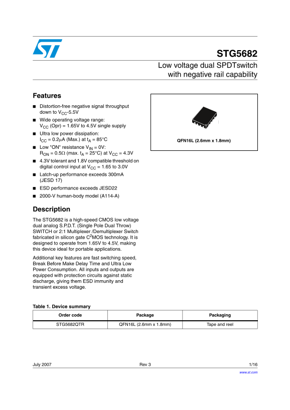
Features Distortion-free negative signal throughput down to VCC-5.5V Wide operating voltage range: VCC (Opr) = 1.65V to 4.5V single supply Ultra low power dissipation: ICC = 0.2µA (Max.) at t A = 85°C

QFN16L (2.6mm x 1.8mm)

Low "ON" resistance VIN = 0V: RON = 0.5Ω (max. t A = 25°C) at VCC = 4.3V 4.3V tolerant and 1.8V compatible threshold on digital control input at VCC = 1.65 to 3.0V Latch-up performance exceeds 300m A (JESD 17) ESD performance exceeds JESD22 2000-V human-body model (A114-A)

Description The STG5682 is a high-speed CMOS low voltage dual analog S.P.D.T. (Single Pole Dual Throw) SWITCH or 2:1 Multiplexer /Demultiplexer Switch fabricated in silicon gate C2MOS technology. It is designed to operate from 1.65V to 4.5V, making this device ideal for portable applications. Additional key features are fast switching speed, Break Before Make Delay Time and Ultra Low Power Consumption. All inputs and outputs are equipped with protection circuits against static discharge, giving them ESD immunity and transient excess voltage.

Table 1. Device summary

Order code Package Packaging

STG5682QTR QFN16L (2.6mm x 1.8mm) Tape and reel

July 2007 Rev 3 1/16

www.st.com

Page Summary Contents For ST STG5682 Low-voltage Dual SPDT Switch with Negative Rail Capability

Page 1 STG5682 Low voltage dual SPDTswitch with negative rail capability Features Distortion-free negative signal throughput down to VCC-5.5V Wide operating voltage range: VCC (Opr) = 1.65V to 4.5V single su...
Page 2 Contents STG5682 Contents Pin settings . . . . . . . . . . . . . . . . . . . . . . . . . . . . . . . . . . . . . . . . . . . . . . . . 3 1.1 Pin connection . . . . . . . . . . . . . . . . . . . . . . ...
Page 3 STG5682 Pin settings 1 Pin settings 1.1 Pin connection Figure 1. Pin connection (top through view) 1SEL 2S2 1S1 2SEL 1.2 Pin description Table 2. Pin description Pin N° Symbol Name and function 4, 2, ...
Page 4 Device summary STG5682 2 Device summary Figure 2. Input equivalent circuit Table 3. Truth table SEL Switch S1 Switch S2 OFF (1) ON OFF (1) 1. High Impedance
Page 5 STG5682 Maximum rating 3 Maximum rating Stressing the device above the rating listed in the “Absolute Maximum Ratings” table may cause permanent damage to the device. These are stress ratings only and...
Page 6 Maximum rating STG5682 3.1 Recommended operating conditions Table 5. Recommended operating conditions Symbol Parameter Value Unit VCC 1.65 to 4.5 Supply voltage(1) VI Input voltage VCC -5.5 to VCC VIC...
Page 7 STG5682 Electrical characteristics 4 Electrical characteristics Table 6. DC specifications Test conditions Value Symbol Parameter TA = 25°C -40 to 85°C Unit Vcc (V) Min Typ Max Min Max 1.65 -1.95 0.65...
Page 8 Electrical characteristics STG5682 Table 6. DC specifications (continued) Test conditions Value Symbol Parameter TA = 25°C -40 to 85°C Unit Vcc (V) Min Typ Max Min Max D ON State VS = Open ID Leakage ...
Page 9 STG5682 Electrical characteristics Table 7. AC electrical characteristics (CL = 35p F, RL = 50Ω, tr = tf ≤ 5ns) Test conditions Value Symbol Parameter TA = 25°C -40 to 85°C Unit Vcc (V) Min Typ Max Mi...
Page 10 Electrical characteristics STG5682 Table 8. Analog switch characteristics (CL = 5p F, RL = 50Ω, TA = 25°C) Test conditions Value Symbol Parameter TA = 25°C -40 to 85°C Unit Vcc (V) Min Typ Max Min Max...
Page 11 STG5682 Package mechanical data 5 Package mechanical data In order to meet environmental requirements, ST offers these devices in ECOPACK® packages. These packages have a Lead-free second level interc...
Page 12 Package mechanical data STG5682 Table 9. QFN16L (2.6x1.8mm) mechanical data Min Typ Max Note: VFQFPN - Standard for thermally enhanced vey fine pitch quad flat package no leads. The leads size is comp...
Page 13 STG5682 Package mechanical data Figure 4. Package information
Page 14 Package mechanical data STG5682 Figure 5. QFN16L (2.6mmx1.8mm) tape & reel
Page 15 STG5682 Revision history 6 Revision history Table 10. Revision history Date Revision Changes 15-Mar-2007 First release 16-Apr-2007 Typo in cover page 05-Jul-2007 Table 6 on page 7 updated
Page 16 STG5682 Please Read Carefully: Information in this document is provided solely in connection with ST products. STMicroelectronics NV and its subsidiaries (“ST”) reserve the right to make changes, corr...

Manual Details

Brand Dual
Pages 16
File Size 219.30 KB
Published May 30, 2026
62 views

Enter the captcha to get the download link:

captcha

Frequently Asked Questions

What voltage range does the STG5682 operate optimally in?

The device operates from 1.65V to 4.5V using a single supply CC.

Can this switch handle negative voltages on signals?

Yes, it provides distortion-free negative signal throughput down to V-5.5V CC.

What is the typical power consumption of the component?

It features ultra low power dissipation, specified at 0.2µA (Max.) at 85°C CC.

Does the device protect against electrical surges?

All inputs and outputs are equipped with protection circuits providing ESD immunity and transient excess voltage handling.