ST STG3682 Low voltage high bandwidth dual SPDT switch Data Sheet
Summary
This high-speed CMOS switch functions as a low voltage dual SPDT selector or 2:1 multiplexer, perfectly designed for connecting signals in sensitive portable equipment. Featuring ultra-low power dissipation and compatibility with USB 2.0 standards, it delivers reliable switching across an extensive operating range (1.65V to 4.3V), all while offering robust ESD protection. The accompanying manual provides developers with complete technical specifications, detailing pin connections, electrical characteristics, and maximum ratings necessary for seamless hardware integration into complex electronic designs.
Page 1 Text Content
STG3682
Low voltage high bandwidth dual SPDT switch
Features Ultra low power dissipation: ICC = 0.2µA (Max.) at TA = 85°C Low “ON” resistance: RON = 4.6Ω (TA = 25°C) at VCC = 4.3V RON = 5.8Ω (TA = 25°C) at VCC = 3.0V
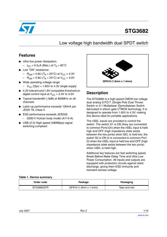
QFN10 (1.8mm x 1.4mm)
Wide operating voltage range: VCC (Opr) = 1.65V to 4.3V single supply 4.3V tolerant and 1.8V compatible threshold on
Description
digital control input at VCC = 2.3V to 3.0V Typical bandwidth (-3d B) at 800MHz on all The STG3682 is a high-speed CMOS low voltage channels dual analog S.P.D.T. (Single Pole Dual Throw)
Switch or 2:1 Multiplexer /Demultiplexer Switch
Latch-up performance exceeds 100m A per
fabricated in silicon gate C2MOS technology. It is
JESD 78, Class II
designed to operate from 1.65V to 4.3V, making
ESD performance exceeds JESD22
this device ideal for portable applications.
2000-V Human body model (A114-A)
The n SEL inputs are provided to control the
USB (2.0) High speed (480Mbps) signal
switch. The switch S1 is ON (they are connected
switching compliant
to common Ports Dn) when the n SEL input is held high and OFF (high impedance state exists between the two ports) when SEL is held low; the switch S2 is ON (it is connected to common Port D) when the n SEL input is held low and OFF (high impedance state exists between the two ports) when n SEL is held high. Additional key features are fast switching speed, Break Before Make Delay Time and Ultra Low Power Consumption. All inputs and outputs are equipped with protection circuits against static discharge, giving them ESD immunity and transient excess voltage.
Table 1. Device summary
Order code Package Packaging
STG3682QTR QFN10 (1.8mm x 1.4mm) Tape and reel
July 2007 Rev 2 1/19
www.st.com
Page Summary Contents For ST STG3682 Low voltage high bandwidth dual SPDT switch Data Sheet
Manual Details
| Brand | Dual |
|---|---|
| Pages | 19 |
| File Size | 330.97 KB |
| Published | May 31, 2026 |
Enter the captcha to get the download link:

Frequently Asked Questions
What is the recommended operating voltage range?
The device operates from 1.65V to 4.3V on a single supply.
How does the nSEL input control switching for S1 and S2?
S1 is ON when nSEL is high; S2 is ON when nSEL is low. Both are OFF (high impedance) otherwise.
What is the junction's ESD protection capability?
It achieves ESD performance exceeding the JESD2000-V Human body model standard.
Is this switch suitable for USB signal switching?
Yes, it can switch high-speed USB (2.0) signals up to 480Mbps.