Fairchild NC7SB3157, FSA3157 Low-Voltage SPDT Analog Switch User Manual
Summary
Designed for modern electronics, the NC7SB3157/FSA3157 is a high-performance, low-voltage SPDT analog switch and 2:1 multiplexer bus switch. Featuring space-saving MicroPak™ packaging, low on resistance (<10Ω), and broad operating ranges (1.65V to 5.5V), it ensures reliable signal handling in both analog and digital applications. This manual provides comprehensive technical documentation, including detailed electrical characteristics, absolute maximum ratings, pin assignments, dimensions, and design guidelines needed by hardware engineers integrating robust bus switching solutions into their circuitry.
Page 1 Text Content
7SB 3157, FSA 3157 — Low -Voltage SPD T A nalog Sw itch or 2:1 M ultiplexer / D e-m ultiplexer B us Sw itch
September 2008
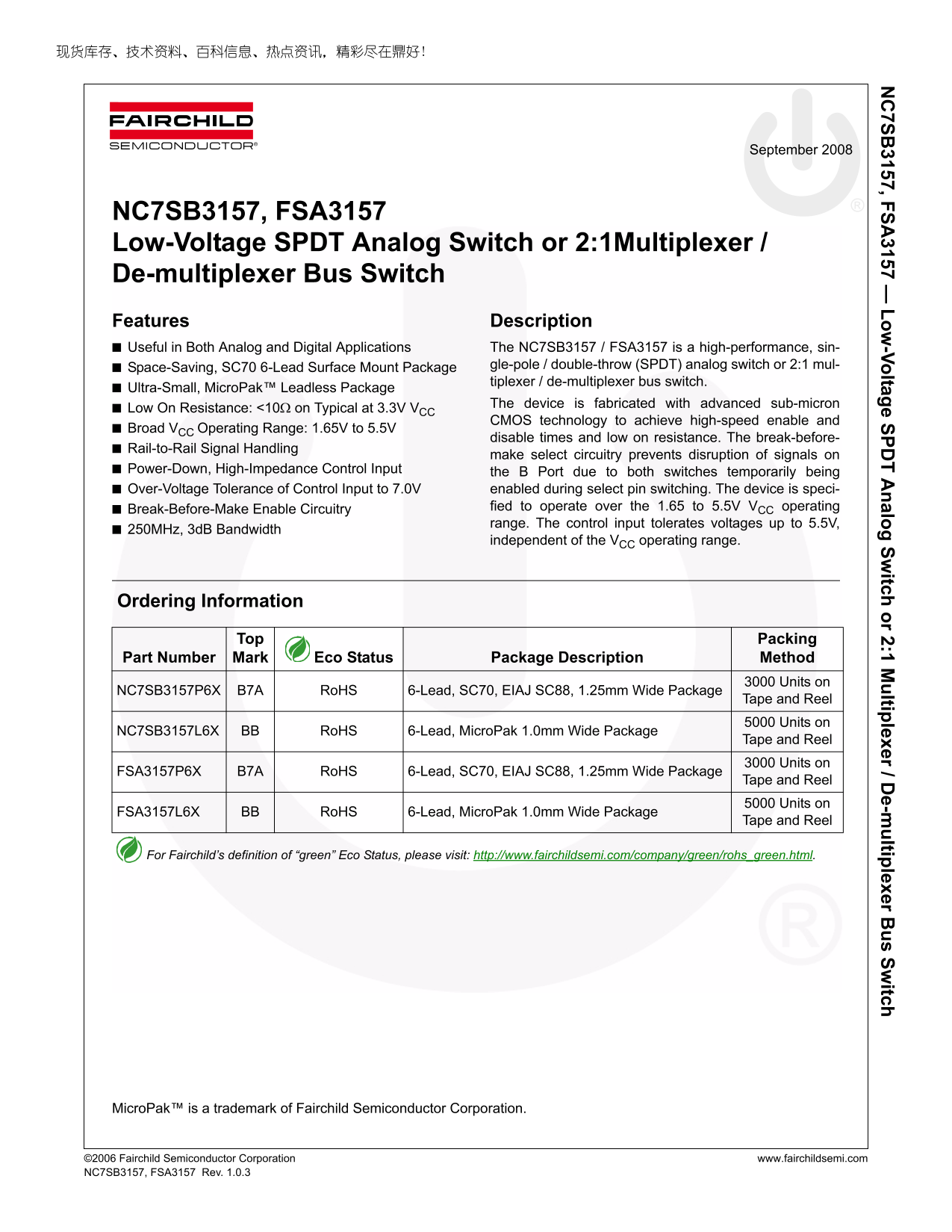
NC7SB3157, FSA3157 Low-Voltage SPDT Analog Switch or 2:1Multiplexer / De-multiplexer Bus Switch Features Description Useful in Both Analog and Digital Applications The NC7SB3157 / FSA3157 is a high-performance, sin-
Space-Saving, SC70 6-Lead Surface Mount Package gle-pole / double-throw (SPDT) analog switch or 2:1 mul- tiplexer / de-multiplexer bus switch.
Ultra-Small, Micro Pak™ Leadless Package
The device is fabricated with advanced sub-micron
Low On Resistance: <10Ω on Typical at 3.3V VCC
CMOS technology to achieve high-speed enable and
Broad VCC Operating Range: 1.65V to 5.5V
disable times and low on resistance. The break-before-
Rail-to-Rail Signal Handling
make select circuitry prevents disruption of signals on
Power-Down, High-Impedance Control Input the B Port due to both switches temporarily being Over-Voltage Tolerance of Control Input to 7.0V enabled during select pin switching. The device is speci-
Break-Before-Make Enable Circuitry fied to operate over the 1.65 to 5.5V VCC operating range. The control input tolerates voltages up to 5.5V,
250MHz, 3d B Bandwidth
independent of the VCC operating range.
Ordering Information
Packing
Part Number Mark Eco Status Package Description Method
3000 Units on
NC7SB3157P6X B7A Ro HS 6-Lead, SC70, EIAJ SC88, 1.25mm Wide Package
Tape and Reel 5000 Units on
NC7SB3157L6X BB Ro HS 6-Lead, Micro Pak 1.0mm Wide Package
Tape and Reel 3000 Units on
FSA3157P6X B7A Ro HS 6-Lead, SC70, EIAJ SC88, 1.25mm Wide Package
Tape and Reel 5000 Units on
FSA3157L6X BB Ro HS 6-Lead, Micro Pak 1.0mm Wide Package
Tape and Reel
For Fairchild’s definition of “green” Eco Status, please visit: http://www.fairchildsemi.com/company/green/rohs_green.html.
Micro Pak™ is a trademark of Fairchild Semiconductor Corporation.
©2006 Fairchild Semiconductor Corporation www.fairchildsemi.com NC7SB3157, FSA3157 Rev. 1.0.3
Page Summary Contents For Fairchild NC7SB3157, FSA3157 Low-Voltage SPDT Analog Switch User Manual
Manual Details
| Brand | Fairchild |
|---|---|
| Pages | 11 |
| File Size | 1.12 MB |
| Published | July 22, 2026 |
Enter the captcha to get the download link:

Frequently Asked Questions
What is the primary function of the NC7SB3157/FSA3157?
It is a high-performance single-pole / double-throw (SPDT) analog switch or 2:1 multiplexer/demultiplexer bus switch useful in both analog and digital applications.
What are the recommended operating conditions for the device's supply voltage and temperature?
The operating supply voltage range is 1.65V to 5.50V, and the temperature range is -40°C to +85°C.
How low is the on-resistance of the switch at typical usage (3.3V)?
The on-resistance is specified as <10Ω typically at 3.3V VCC.
Which package types are available for this component?
It is available in both SC70 and MicroPak™ Leadless packages, with MicroPak offering a width of 1.0mm.