Fairchild NC7SB3157, FSA3157 Low Voltage SPDT Analog Switch or 2x1 Multiplexer/Demultiplexer/Bus Switch Owner's Manual
Summary
This comprehensive guide details the NC7SB3157/FSA3157, a high-performance, ultra-small SPDT Analog Switch and 2:1 Multiplexer designed for both analog and digital circuits. The manual provides critical technical specifications, including low on resistance (< 10Ω), broad operating ranges (1.65V to 5.5V), and detailed pin assignments. It covers absolute maximum ratings, recommended operating conditions, and ordering details, making it an essential resource for electronics engineers and system designers integrating reliable signal switching components into advanced circuit boards.
Page 1 Text Content
7S 3157, F 3157 L Vo ltag e S alo itch r 2:1 M ltip lexer/D em ltip lexer B s S itch
March 2006
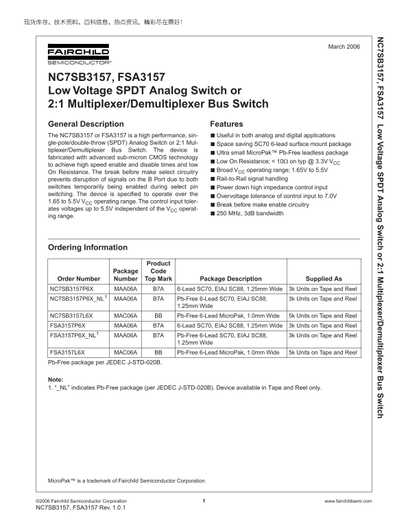
NC7SB3157, FSA3157 Low Voltage SPDT Analog Switch or 2:1 Multiplexer/Demultiplexer Bus Switch General Description Features The NC7SB3157 or FSA3157 is a high performance, sin- Useful in both analog and digital applications gle-pole/double-throw (SPDT) Analog Switch or 2:1 Mul- Space saving SC70 6-lead surface mount package tiplexer/Demultiplexer Bus Switch. The device is
Ultra small Micro Pak™ Pb-Free leadless package
fabricated with advanced sub-micron CMOS technology
Low On Resistance; < 10 on typ @ 3.3V V
to achieve high speed enable and disable times and low
Broad V operating range; 1.65V to 5.5V On Resistance. The break before make select circuitry CC prevents disruption of signals on the B Port due to both Rail-to-Rail signal handling
switches temporarily being enabled during select pin Power down high impedance control input switching. The device is specified to operate over the
Overvoltage tolerance of control input to 7.0V
1.65 to 5.5V V operating range. The control input toler-
Break before make enable circuitry
ates voltages up to 5.5V independent of the V operat-
250 MHz, 3d B bandwidth
ing range.
Ordering Information
Product Package Code Order Number Number Top Mark Package Description Supplied As
NC7SB3157P6X MAA06A B7A 6-Lead SC70, EIAJ SC88, 1.25mm Wide 3k Units on Tape and Reel NC7SB3157P6X_NL MAA06A B7A Pb-Free 6-Lead SC70, EIAJ SC88, 3k Units on Tape and Reel
1.25mm Wide
NC7SB3157L6X MAC06A BB Pb-Free 6-Lead Micro Pak, 1.0mm Wide 5k Units on Tape and Reel FSA3157P6X MAA06A B7A 6-Lead SC70, EIAJ SC88, 1.25mm Wide 3k Units on Tape and Reel
FSA3157P6X_NL MAA06A B7A Pb-Free 6-Lead SC70, EIAJ SC88, 3k Units on Tape and Reel
1.25mm Wide
FSA3157L6X MAC06A BB Pb-Free 6-Lead Micro Pak, 1.0mm Wide 5k Units on Tape and Reel Pb-Free package per JEDEC J-STD-020B.
Note: 1. “_NL” indicates Pb-Free package (per JEDEC J-STD-020B). Device available in Tape and Reel only.
Micro Pak™ is a trademark of Fairchild Semiconductor Corporation.
©2006 Fairchild Semiconductor Corporation www.fairchildsemi.com NC7SB3157, FSA3157 Rev. 1.0.1
Page Summary Contents For Fairchild NC7SB3157, FSA3157 Low Voltage SPDT Analog Switch or 2x1 Multiplexer/Demultiplexer/Bus Switch Owner's Manual
Manual Details
| Brand | Fairchild |
|---|---|
| Pages | 14 |
| File Size | 562.47 KB |
| Published | May 20, 2026 |
Enter the captcha to get the download link:

Frequently Asked Questions
What voltage range should I operate this SPDT Analog Switch within?
The specified operating voltage range is 1.65V to 5.5V DC.
Are there any limitations on using this device in critical systems?
No, the product is not authorized for use as critical components in life support devices without express written approval.
What must I ensure about the control input signal when operating the switch?
The control input must be held HIGH or LOW; it must not float.
How is this device packaged and supplied to customers?
The device is available only in Tape and Reel format.