MAXIM MAX394 Low-Voltage, Quad, SPDT, CMOS Analog Switch Data Sheet - User Manual
Summary
The MAX394 is a highly reliable, low-voltage, quad Single-Pole Double-Throw (SPDT) analog switch designed for critical signal routing applications. This CMOS/TTL compatible device features ultra-low on-resistance and guaranteed signal fidelity across both single and bipolar supply ranges. The manual details comprehensive specifications, including various packaging options, operating temperature ranges, and electrical testing data. It is ideal for engineers designing portable instruments, audio equipment, communications systems, or set-top display interfaces requiring precise power management switching.
Page 1 Text Content
19-0391; Rev 2; 9/08
Low-Voltage, Quad, SPDT, CMOS Analog Switch
_______________General Description ____________________________Features
The MAX394 is a precision, low-voltage, quad, single- Low On-Resistance, < 17Ω Typical (35Ω max) pole/double-throw (SPDT) analog switch. The four inde- Guaranteed Matched On-Resistance Between pendent switches operate with bipolar supplies ranging Channels, < 2Ω from ±2.7V to ±8V, or with a single supply of +2.7V to Guaranteed Flat On-Resistance over Analog Signal Range, Δ4Ω Max
+15V. The MAX394 offers low on-resistance (less than
35Ω), guaranteed to match within 2Ω between channels Guaranteed Charge Injection < 10p C
and to remain flat over the analog signal range (Δ4Ω Guaranteed Off-Channel Leakage < 2.5n A at +85°C max). It also offers break-before-make switching (10ns
ESD Guaranteed > 2000V per Method 3015.7
typical), with turn-off times less than 75ns and turn-on
Single-Supply Operation (+2.7V to +15V)
times less than 130ns. The MAX394 is ideal for portable
Bipolar-Supply Operation (±2.7V to ±8V)
operation since quiescent current runs less than 1µA with
TTL/CMOS-Logic Compatibility
all inputs high or low.
Rail-to-Rail Analog Signal Handling Capability
This monolithic, quad switch is fabricated with Maxim’s
Pin Compatible with MAX333, MAX333A
low voltage silicon-gate process. Design improvements
guarantee extremely low charge injection (10p C), low Ordering Information
power consumption (10µW), and electrostatic discharge
PART TEMPERATURE PIN-PACKAGE
(ESD) greater than 2000V.
MAX394CPP 0°C to +70°C 20 Plastic DIP
Logic inputs are TTL and CMOS compatible and guaran-
teed over a +0.8V to +2.4V range for supply voltages up MAX394CWP 0°C to +70°C 20 Wide SO
to +8V. When supplies exceed +8V, the inputs are typi- MAX394C/D 0°C to +70°C Dice* cally +0.8V to +4V. Logic inputs and switched analog sig-
MAX394EPP -40°C to +85°C 20 Plastic DIP
nals can range anywhere between the supply voltages
MAX394EWP -40°C to +85°C 20 Wide SO
without damage.
MAX394EUP -40°C to +85°C 20 TSSOP
________________________Applications
MAX394MJP -55°C to +85°C 20 CERDIP**
Test Equipment Portable Instruments
MAX394MWP/PR -55°C to +125°C 20 Wide SO**
Communications Systems Audio Signal Routing
MAX394MWP/PR-T -55°C to +125°C 20 Wide SO**
PBX, PABX Set-Top Boxes
*Contact factory for dice specifications.
Heads-Up Displays **Contact factory for availability.
Typical Operating Circuit
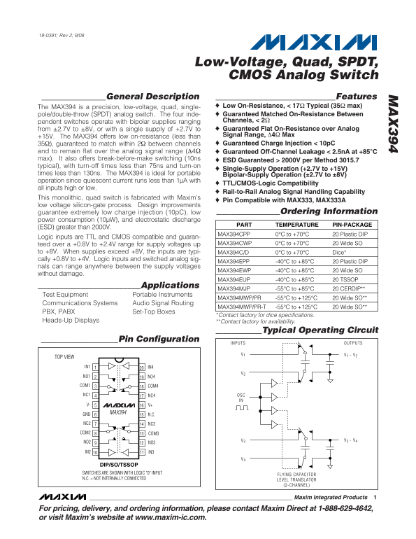
__________________Pin Configuration
INPUTS OUTPUTS
TOP VIEW
IN1 IN4
NO1 NO4
COM1 COM4
NC4NC1 OSC IN
MAX394
GND N.C.
NC2 NC3
COM3COM2
NO2 NO3
IN3IN2
DIP/SO/TSSOP SWITCHES ARE SHOWN WITH LOGIC "0" INPUT
FLYING CAPACITOR
N.C. = NOT INTERNALLY CONNECTED
LEVEL TRANSLATOR (2-CHANNEL)
Maxim Integrated Products
For pricing, delivery, and ordering information, please contact Maxim Direct at 1-888-629-4642, or visit Maxim’s website at www.maxim-ic.com.
Page Summary Contents For MAXIM MAX394 Low-Voltage, Quad, SPDT, CMOS Analog Switch Data Sheet - User Manual
Manual Details
| Brand | QUAD |
|---|---|
| Pages | 13 |
| File Size | 235.80 KB |
| Published | May 27, 2026 |
Enter the captcha to get the download link:

Frequently Asked Questions
Does this switch support bipolar or single supply operation?
Yes, it supports bipolar supplies ranging from ±2.7V to ±8V, or a single supply of +2.7V to +15V.
What is the guaranteed electrical matching across the channels?
It guarantees matched On-Resistance within 2Ω between all channels and maintains flat resistance over the analog signal range (Δ4Ω).
Is this device compatible with common logic signals?
The product's logic inputs are fully TTL and CMOS compatible, regardless of whether they are input high or low.
What is the ESD protection level offered by the MAX394?
It guarantees an Electrostatic Discharge (ESD) rating greater than 2000V per Method 3015.7 typical.