ROHM RSE002P03 Product Specifications
Summary
Discover the RSE002P03 P-channel MOSFET, a high-performance transistor ideal for power switching applications. This comprehensive manual provides detailed technical data, including absolute maximum ratings, electrical characteristics (e.g., On-state resistance, capacitance), and operational guidelines. It is essential documentation for electronic engineers and circuit designers who require reliable specifications for low on-resistance switching components in demanding systems.
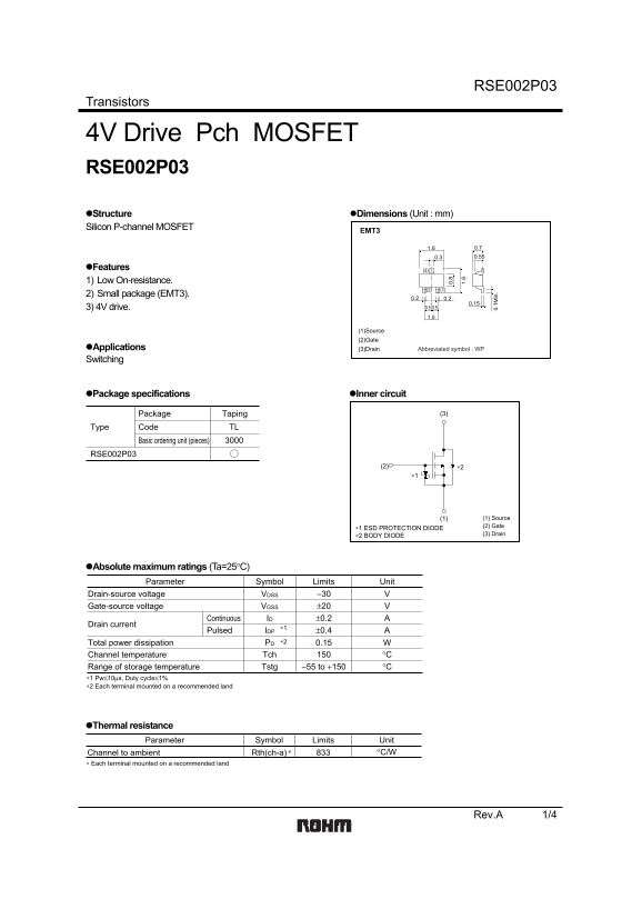
Page 1 Text Content
RSE002P03
Transistors
4V Drive Pch MOSFET RSE002P03 Structure Dimensions (Unit : mm) Silicon P-channel MOSFET
Features (3) 1) Low On-resistance.
2) Small package (EMT3).
3) 4V drive. 0.50.5 1.0
(1)Source (2)Gate
Applications (3)Drain Abbreviated symbol : WP Switching
Package specifications Inner circuit
Package Taping (3)
Type Code TL
Basic ordering unit (pieces)
RSE002P03
0. 1M in
(1) (1) Source (2) Gate
∗1 ESD PROTECTION DIODE
∗2 BODY DIODE (3) Drain
Absolute maximum ratings (Ta=25°C)
Parameter Symbol Limits Unit
Drain-source voltage −30 VVDSS Gate-source voltage ±20 VVGSS
Continuous ±0.2 AID
Drain current
Pulsed ±0.4 AIDP
Total power dissipation ∗2 0.15 WPD
Channel temperature °CTch
Range of storage temperature −55 to +150 °CTstg
∗1 Pw≤10µs, Duty cycle≤1% ∗2 Each terminal mounted on a recommended land
Thermal resistance
Parameter Symbol Limits Unit
Channel to ambient °C/WRth(ch-a)
∗ Each terminal mounted on a recommended land
Rev.A 1/4
Page Summary Contents For ROHM RSE002P03 Product Specifications
Manual Details
| Brand | ROHM |
|---|---|
| Pages | 5 |
| File Size | 63.31 KB |
| Published | May 29, 2026 |
Enter the captcha to get the download link:

Frequently Asked Questions
What is the standard mounting environment for this MOSFET?
The thermal resistance ratings assume that each terminal is mounted on a recommended land.
How low is the maximum on-state resistance (RDS(on))?
At an ID of −0.15A and VGS = −4.5V, the RDS(on) is listed as 1.4 Ohm minimum.
What are the limits for drain-source voltage and gate-source voltage?
The limits are VDSS: −30 V to −30 V, and VGSS: ±20 V.
What precautions should be taken regarding high-reliability applications?
For equipment that directly endangers human life (like medical or aerospace machinery), consult a sales representative.