# A B C D E F G H I J K L M N O P Q R S T U V W X Y Z

RICOH RP401x SERIES STEP-UP DC DC CONVERTERS DATASHEET USER GUIDE

Summary

The RP401x Series offers high-efficiency, small-package step-up DC/DC converters for portable and battery-powered electronics such as MP3 players, PDAs, and digital cameras. Designed to operate reliably from extremely low voltages (as low as 0.6V), these ICs provide stable, adjustable power output between 1.8V and 5.5V. This manual details the core technical specifications, including various operational modes—from fixed PWM output to automatic PWM/VFM shifting—and provides comprehensive guides to assist embedded system designers in selecting the optimal component for their compact energy-efficient needs.
📄 Preview PAGE OF 24

Page 1 Text Content

RP401x SERIES

HIGH EFFICIENCY, SMALL PACKAGES, STEP-UP DC/DC CONVERTERS

NO.EA-260-111009

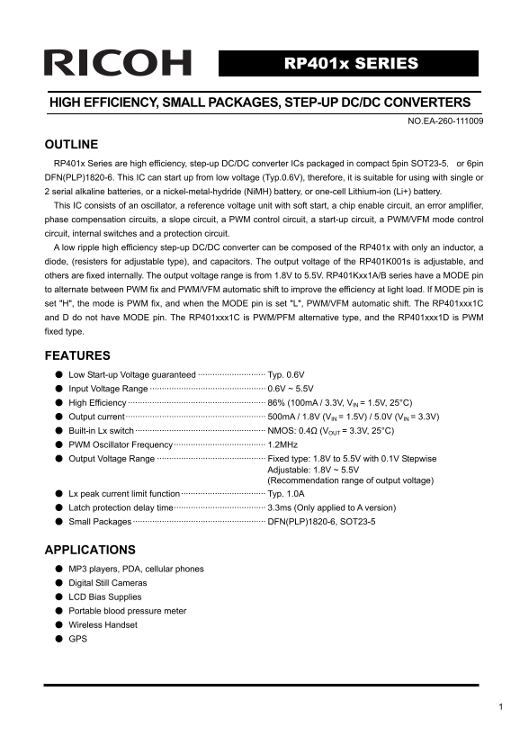
OUTLINE RP401x Series are high efficiency, step-up DC/DC converter ICs packaged in compact 5pin SOT23-5, or 6pin DFN(PLP)1820-6. This IC can start up from low voltage (Typ.0.6V), therefore, it is suitable for using with single or 2 serial alkaline batteries, or a nickel-metal-hydride (Ni MH) battery, or one-cell Lithium-ion (Li+) battery. This IC consists of an oscillator, a reference voltage unit with soft start, a chip enable circuit, an error amplifier, phase compensation circuits, a slope circuit, a PWM control circuit, a start-up circuit, a PWM/VFM mode control circuit, internal switches and a protection circuit. A low ripple high efficiency step-up DC/DC converter can be composed of the RP401x with only an inductor, a diode, (resisters for adjustable type), and capacitors. The output voltage of the RP401K001s is adjustable, and others are fixed internally. The output voltage range is from 1.8V to 5.5V. RP401Kxx1A/B series have a MODE pin to alternate between PWM fix and PWM/VFM automatic shift to improve the efficiency at light load. If MODE pin is set "H", the mode is PWM fix, and when the MODE pin is set "L", PWM/VFM automatic shift. The RP401xxx1C and D do not have MODE pin. The RP401xxx1C is PWM/PFM alternative type, and the RP401xxx1D is PWM fixed type.

FEATURES ● Low Start-up Voltage guaranteed ···························· Typ. 0.6V ● Input Voltage Range ················································ 0.6V ~ 5.5V ● High Efficiency ························································· 86% (100m A / 3.3V, VIN = 1.5V, 25°C) ● Output current·························································· 500m A / 1.8V (VIN = 1.5V) / 5.0V (VIN = 3.3V) ● Built-in Lx switch ······················································ NMOS: 0.4Ω (VOUT = 3.3V, 25°C) ● PWM Oscillator Frequency······································ 1.2MHz ● Output Voltage Range ············································· Fixed type: 1.8V to 5.5V with 0.1V Stepwise Adjustable: 1.8V ~ 5.5V (Recommendation range of output voltage) ● Lx peak current limit function··································· Typ. 1.0A ● Latch protection delay time······································ 3.3ms (Only applied to A version) ● Small Packages ······················································· DFN(PLP)1820-6, SOT23-5

APPLICATIONS ● MP3 players, PDA, cellular phones ● Digital Still Cameras ● LCD Bias Supplies ● Portable blood pressure meter ● Wireless Handset ● GPS

Page Summary Contents For RICOH RP401x SERIES STEP-UP DC DC CONVERTERS DATASHEET USER GUIDE

Page 1 RP401x SERIES HIGH EFFICIENCY, SMALL PACKAGES, STEP-UP DC/DC CONVERTERS NO.EA-260-111009 OUTLINE RP401x Series are high efficiency, step-up DC/DC converter ICs packaged in compact 5pin SOT23-5, or 6pi...
Page 2 RP401x Series BLOCK DIAGRAMS Fixed output; RP401Kxx1A/B OSCILLATOR STARTUP CURRENT CONTROL LX CIRCUIT PROTECTION VREF SWITCHING CONTROL CURRENT START FEEDBACK RAMP COMPENSATION ENABLE MODE CONTROL Adj...
Page 3 RP401x Series Fixed output type: RP401Nxx1C/D VFM CURRENT OSCILLATOR STARTUP CONTROL* LX CIRCUIT PROTECTION VREF SWITCHING CONTROL CURRENT START FEEDBACK RAMP COMPENSATION ENABLE *) Applied to PWM/VFM...
Page 4 RP401x Series Product code table Latch type Version MODE pin Output Voltage over-current package protection A Yes Fixed Yes DFN(PLP)1820-6 B Yes Fixed No DFN(PLP)1820-6 Fixed No SOT-23-5 (PWM/VFM auto...
Page 5 RP401x Series * Tab is GND level. (They are connected to the reverse side of this IC.) Connected to the GND is the recommendation, leaving it open is also possible. RP401Nxx1C/D: SOT-23-5 Pin No Symbo...
Page 6 RP401x Series ELECTRICAL CHARACTERISTICS Adjustable types (RP401K001C/D) (Ta=25°C) Symbol Item Conditions MIN. TYP. MAX. Unit VIN Input Voltage 5.5 V Vstart Start-up Voltage Load current =1m A 0.6 0.8...
Page 7 RP401x Series Fixed output voltage types (RP401Kxx1A/B, RP401Nxx1C/D) (Ta=25°C) Symbol Item Conditions MIN. TYP. MAX. Unit VIN Input Voltage 5.5 V Vstart Start-up Voltage Load current =1m A 0.6 0.8 V ...
Page 8 RP401x Series APPLICATION NOTES Fixed Output Voltage Type (RP401Kxx1A/B) 4.7µH Schottky Diode LX VIN CIN 10µF RP401Kxx1x CE VOUT CE Control MODE Control Adjustable output type (RP401K001C/D) 4.7µH Sch...
Page 9 RP401x Series Fixed output type (RP401Nxx1C/D) 4.7µH Schottky Diode LX VIN CIN 10µF RP401Nxx1x CE COUT CE Control External components Capacitor CIN: C1608JB0J106M (TDK), COUT: VOUT[V] ILmax<700m A ...
Page 10 RP401x Series VOUT pin. Consider the bias shift, choose the enough capacity of the capacitor. A ceramic capacitor (10μF) between VIN and ground should be set. The inductor value recommendation is 4.7μ...
Page 11 RP401x Series OUTPUT CURRENT OF STEP-UP CIRCUIT AND EXTERNAL COMPONENTS <Basic Circuit> Inductor Diode VIN VOUT CL Lx Tr <Current through L> Discontinuous Continuous ILxmax IL IL ILxmax IL...
Page 12 RP401x Series In PWM control, when tf = toff is true, the inductor current becomes continuous, then the operation of switching regulator becomes continuous mode. In the continuous mode, the deviation ...
Page 13 RP401x Series ■ TIMING CHART Soft start operation and Latch protection operation Input Voltage CE Voltage Output Current 1.65V (TYP.) Output Voltage LX Voltage tprot 0.7ms (TYP.) 3.3ms (TYP.) Latch Pr...
Page 14 of t S ta rt er io [m s] RP401x Series Soft Start Period vs. Temperature RP401xxx1x Soft Start Period vs. Input Voltage RP401xxx1x VIN=VSET×0.5, RL=1kΩ IOUT=1m A 3.5 3.5 VSET=1.8V VSET=1.8V VSET=3.3V ...
Page 15 ut pu t V ol ta ge [V ut pu t V olt ag [V RP401x Series ut pu t V olt ag [V TYPICAL CHARACTERISTICS 1) Output voltage vs. output current (Ta=25°C) RP401K001x RP401K001x VOUT=1.8V VOUT=1.8V RP401x181x ...
Page 16 ffi ci en cy Ef fic ie nc ut pu t V olt ag [V RP401x Series RP401K001x RP401K001x VOUT=5.5V RP401x551x VOUT=5.5V RP401x551x MODE=H MODE=L VI N=0. 7V VIN=0.7V 5.40 VI N=0. 8V VIN=0.8V VI N=1. 5V VIN=1....
Page 17 St an by ur re nt [u ffi ci en cy RP401x Series ffic ie nc RP401K001x RP401K001x VOUT=5.0V RP401x501x RP401x501x VOUT=5.0V MODE=L MODE=H VIN=0.7V VIN=0.7V VIN=0.8V VIN=0.8V VIN=0.9V VIN=0.9V VIN=1.2V ...
Page 18 of t S ta rt Pe rio [m s] IN [V ID D2 [µ A] RP401x Series 5) Supply Current 2 vs. Temperature RP401K001C RP401K001D RP401x331A/B/C RP401N331D VOUT=3.3V VOUT=3.3V Ta [°C] Ta [°C] of t S ta rt Pe rio [m...
Page 19 IL xp ea [m IL xp ea [m RP401x Series fo sc [k z] 10) Frequency vs. Temperature 11) Maximum duty cycle vs. Temperature RP401K001x RP401K001x RP401x331x RP401x331x VOUT=3.3V OUT=3.3V Ta [°C] Ta [°C] 12...
Page 20 CE [V IL xp ea [m A] IL xp ea [m A] RP401x Series 13) Lx Current limit vs. Temperature RP401K001x VOUT=1.8V RP401K001x VOUT=3.3V RP401x181x RP401x331x IN=0.7V VIN=1.0V VIN=0.7V VIN=1.5V VIN=1.0V VIN=2...
Page 21 ut pu t V ol ta ge [V Vo lta ge [V RP401x Series ut pu t V ol ta ge [V 16) Output voltage vs. Temperature 17) Feedback voltage vs. Temperature RP401x331x RP401K001x In tp ut ur re nt [A Ta [°C] Ta [°C...
Page 22 ut pu t V ol ta ge [V ut pu t V ol ta ge [V IL xp ea [m A] RP401x Series 20) Output voltage waveform (Ta=25°C) RP401K001C VOUT=3.3V VIN=1.5V RP401K001D VOUT=3.3V VIN=1.5V RP401x331x IOUT=1m A MODE=L R...
Page 23 ut pu t V ol ta ge [V RP401x Series 22) Mode alternative waveform (Ta=25°C) RP401K331A/B RP401K331A/B VIN=1.5V IOUT=0.1m A VIN=1.5V IOUT=0.1m A MODE Input Voltage MODE Input Voltage Output Voltage 3.2...
Page 24 1. The products and the product specifications described in this document are subject to change or discontinuation of production without notice for reasons such as improvement. Therefore, before decid...

Manual Details

Brand Ricoh
Pages 24
File Size 575.77 KB
Published May 29, 2026
69 views

Enter the captcha to get the download link:

captcha

Frequently Asked Questions

Can this converter operate with low-voltage batteries?

Yes, it guarantees a low start-up voltage (Typ. 0.6V), making it suitable for single or two-series alkaline/NiMH/Li+ batteries.

How do I select the optimal mode for efficiency?

The MODE pin can be set to "L" (PWM/VFM automatic shift) for improved light load efficiency, or choose version 'C' which is a PWM/VFM alternative type.

Does this product have adjustable output voltage?

Yes. The output voltage ranges from 1.8V to 5.5V and can be adjusted on certain versions; others are fixed internally.

What protective features are included with the converter?

It includes a built-in Lx switch, and depending on the model version (A or B), it offers latch type over-current protection circuitry.