RICOH R1210Nxx1x SERIES PWM STEP-UP DC DC CONVERTER
Summary
The R1210Nxx1x Series is a high-accuracy, CMOS-based PWM Step-Up DC/DC Converter designed for mission-critical portable electronics. Optimized for battery-powered devices—including cameras, communication gear, and specialized appliances—it delivers low ripple and exceptional efficiency while minimizing external components to just an inductor, diode, and capacitor. Featuring built-in transient load detection and ultra-low standby current (down to 0.5μA), this converter ensures stable power boosting for applications requiring precise voltage regulation above the battery voltage level.
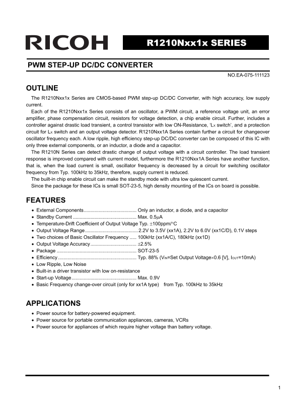
Page 1 Text Content
R1210Nxx1x SERIES
PWM STEP-UP DC/DC CONVERTER
NO.EA-075-111123
OUTLINE The R1210Nxx1x Series are CMOS-based PWM step-up DC/DC Converter, with high accuracy, low supply current. Each of the R1210Nxx1x Series consists of an oscillator, a PWM circuit, a reference voltage unit, an error amplifier, phase compensation circuit, resistors for voltage detection, a chip enable circuit. Further, includes a controller against drastic load transient, a control transistor with low ON-Resistance, ‘LX switch’, and a protection circuit for LX switch and an output voltage detector. R1210Nxx1A Series contain further a circuit for changeover oscillator frequency each. A low ripple, high efficiency step-up DC/DC converter can be composed of this IC with only three external components, or an inductor, a diode and a capacitor. The R1210N Series can detect drastic change of output voltage with a circuit controller. The load transient response is improved compared with current model, furthermore the R1210Nxx1A Series have another function, that is, when the load current is small, oscillator frequency is decreased by a circuit for switching oscillator frequency from Typ. 100k Hz to 35k Hz, therefore, supply current is reduced. The built-in chip enable circuit can make the standby mode with ultra low quiescent current. Since the package for these ICs is small SOT-23-5, high density mounting of the ICs on board is possible.
FEATURES • External Components....................................... Only an inductor, a diode, and a capacitor • Standby Current Max. 0.5μA • Temperature-Drift Coefficient of Output Voltage Typ. ±100ppm/°C • Output Voltage Range....................................... 2.2V to 3.5V (xx1A), 2.2V to 6.0V (xx1C/D), 0.1V steps • Two choices of Basic Oscillator Frequency 100k Hz (xx1A/C), 180k Hz (xx1D) • Output Voltage Accuracy.................................. ±2.5% • Package SOT-23-5 • Efficiency Typ. 88% (VIN=Set Output Voltage×0.6 [V], IOUT=10m A) • Low Ripple, Low Noise • Built-in a driver transistor with low on-resistance • Start-up Voltage................................................ Max. 0.9V • Basic Frequency change-over circuit (only for xx1A type) from Typ. 100k Hz to 35k Hz
APPLICATIONS • Power source for battery-powered equipment. • Power source for portable communication appliances, cameras, VCRs • Power source for appliances of which require higher voltage than battery voltage.
Page Summary Contents For RICOH R1210Nxx1x SERIES PWM STEP-UP DC DC CONVERTER
Manual Details
| Brand | Ricoh |
|---|---|
| Pages | 17 |
| File Size | 305.49 KB |
| Published | June 04, 2026 |
Enter the captcha to get the download link:

Frequently Asked Questions
What external components are needed for the DC/DC converter?
It can operate using only an inductor, a diode, and a capacitor of external components.
How does the R1210Nxx1A series save power when operating with low load current?
It uses a frequency change-over circuit to decrease the oscillator frequency from Typ. 100kHz to 35kHz.
What is the maximum standby current of this converter?
The built-in chip enable circuit allows for ultra low quiescent current, with a max standby current of 0.5μA.
What is the typical operating temperature range for the R1210Nxx1x series?
The device has an operational temperature range from -40 to 85 °C.