# A B C D E F G H I J K L M N O P Q R S T U V W X Y Z

RICOH R1211x SERIES PWM STEP-UP DC DC CONTROLLER

Summary

The R1211x Series is a high-efficiency, CMOS-based PWM step-up DC/DC controller ideal for creating stable constant voltage power sources in portable electronic equipment. This technical manual provides comprehensive details on the integrated circuit's functionality, including internal soft start and latch-type protection circuits. It covers various operational specifications (input range, oscillator frequency), selection guide nuances, pin configurations, and performance data necessary for engineers designing reliable powered systems like LCD or CCD constant voltage supplies.
📄 Preview PAGE OF 36

Page 1 Text Content

R1211x SERIES

PWM STEP-UP DC/DC CONTROLLER

NO.EA-088-120201

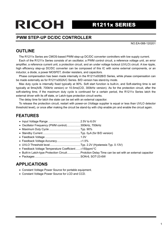
OUTLINE The R1211x Series are CMOS-based PWM step-up DC/DC converter controllers with low supply current. Each of the R1211x Series consists of an oscillator, a PWM control circuit, a reference voltage unit, an error amplifier, a reference current unit, a protection circuit, and an under voltage lockout (UVLO) circuit. A low ripple, high efficiency step-up DC/DC converter can be composed of this IC with some external components, or an inductor, a diode, a power MOSFET, divider resisters, and capacitors. Phase compensation has been made internally in the R1211x002B/D Series, while phase compensation can be made externally as for R1211x002A/C Series. B/D version has stand-by mode. Max duty cycle is internally fixed typically at 90%. Soft start function is built-in, and Soft-starting time is set typically at 9ms(A/B, 700k Hz version) or 10.5ms(C/D, 300k Hz version). As for the protection circuit, after the soft-starting time, if the maximum duty cycle is continued for a certain period, the R1211x Series latch the external driver with its off state, or Latch-type protection circuit works. The delay time for latch the state can be set with an external capacitor. To release the protection circuit, restart with power-on (Voltage supplier is equal or less than UVLO detector threshold level), or once after making the circuit be stand-by with chip enable pin and enable the circuit again.

FEATURES • Input Voltage Range .........................................2.5V to 6.0V • Oscillator Frequency (PWM control).................300k Hz, 700k Hz • Maximum Duty Cycle ........................................Typ. 90% • Standby Current ................................................Typ. 0μA (for B/D version) • Feedback Voltage .............................................1.0V • Feedback Voltage Accuracy..............................±1.5% • UVLO Threshold level.......................................Typ. 2.2V (Hysteresis Typ. 0.13V) • Feedback Voltage Temperature Coefficient ......±150ppm/°C • Built-in Latch-type Protection Circuit.................Protction Delay Time can be set with an external capacitor • Packages ..........................................................SON-6, SOT-23-6W

APPLICATIONS • Constant Voltage Power Source for portable equipment. • Constant Voltage Power Source for LCD and CCD.

Page Summary Contents For RICOH R1211x SERIES PWM STEP-UP DC DC CONTROLLER

Page 1 R1211x SERIES PWM STEP-UP DC/DC CONTROLLER NO.EA-088-120201 OUTLINE The R1211x Series are CMOS-based PWM step-up DC/DC converter controllers with low supply current. Each of the R1211x Series consists...
Page 2 BLOCK DIAGRAMS Version A/C Version B/D OSC OSC VFB EXT DTC VFB EXT AMPOUT VIN Vref GND Vref UVLO UVLO DELAY DELAY Latch Latch Enable SELECTION GUIDE In the R1211x Series, the oscillator frequency, the...
Page 3 PIN CONFIGURATIONS SON-6 SOT-23-6W Top View Bottom View 5 4 (mark side) PIN DESCRIPTIONS Pin No R1211x002A/C R1211x002B/D Symbol Pin Description SON-6 SOT-23-6W SON-6 SOT-23-6W DELAY 1 1 1 1 Pin for E...
Page 4 ABSOLUTE MAXIMUM RATINGS Symbol Item Rating Unit VIN VIN Pin Voltage 6.5 V VEXT EXT Pin Output Voltage −0.3 ~ VIN+0.3 V VDLY DELAY Pin Voltage −0.3 ~ VIN+0.3 V VAMP AMPOUT Pin Voltage −0.3 ~ VIN+0.3 V...
Page 5 ELECTRICAL CHARACTERISTICS • R1211x002A Topt=25°C Symbol Item Conditions Min. Typ. Max. Unit VIN Operating Input Voltage 2.5 6.0 V VFB Feedback Voltage VIN=3.3V 0.985 1.000 1.015 ΔVFB/ΔTopt VFB Voltag...
Page 6 Topt=25°C Symbol Item Conditions Min. Typ. Max. Unit VIN Operating Input Voltage 2.5 6.0 V VFB Feedback Voltage VIN=3.3V 0.985 1.000 1.015 ΔVFB/ΔTopt VFB Voltage Temperature Coefficient −40°C ≤ Topt ≤...
Page 7 Topt=25°C Symbol Item Conditions Min. Typ. Max. Unit VIN Operating Input Voltage 2.5 6.0 V VFB VFB Voltage Tolerance VIN=3.3V 0.985 1.000 1.015 ΔVFB/Δ VFB Voltage Topt Temperature Coefficient −40°C ≤ ...
Page 8 Topt=25°C Symbol Item Conditions Min. Typ. Max. Unit VIN Operating Input Voltage 2.5 6.0 V VFB VFB Voltage Tolerance VIN=3.3V 0.985 1.000 1.015 ΔVFB/Δ VFB Voltage Topt Temperature Coefficient −40°C ≤ ...
Page 9 TYPICAL APPLICATIONS AND TECHNICAL NOTES Inductor VOUTDiode VIN EXT DELAY C3 GND AMPOUT NMOS : IRF7601 (International Rectifier) Inductor: LDR655312T-100 10μH (TDK) for R1211x002A : LDR655312T-220 22...
Page 10 Use a 1μF or more capacitance value of bypass capacitor between VIN pin and GND, C1 as shown in the typical applications above. • In terms of the capacitor for setting delay time of the latch protecti...
Page 11 Output Current and Selection of External Components <Basic Circuit> Inductor Diode IOUT VIN VOUT CLLX Tr <Circuit through L> Discontinuous Mode Continuous Mode IL IL ILxmax ILxmax ILxmin I...
Page 12 When IOUT becomes more than formula 5, the current flows through the inductor, then the mode becomes continuous. The continuous current through the inductor is described as Iconst, then, INOSCOUT ON ×...
Page 13 TIMING CHART • R1211x002A/R1211x002C DTC SS VOUT AMPOUT PWM Comparator OP AMP DTC SS VOUT AMPOUT PWM Comparator OP AMP <Soft-start Operation> Soft-start operation is starting from power-on as fo...
Page 14 (Step3) When SS reaches 1V, soft-start operation finishes. VREF becomes constant voltage (=1V). Then the switching operation becomes normal mode. SS,VREF VFB,VREF DTC AMPOUT AMPOUT Step1 Step2 Step3 &...
Page 15 TEST CIRCUITS ∗Oscillator Frequency, Maximum Duty Cycle, VFB Voltage Test ∗Consumption Current Test VIN EXT OSCILLOSCOPE GND DELAY GND DELAY ∗EXT "H" ON Resistance ∗EXT "L" ON Resi...
Page 16 ∗DELAY Pin Detector Threshold Voltage Test ∗AMP "H" Output Current/"L" Output Current Test VIN EXT VIN OSCILLOSCOPE AMPOUT VFB VFB GND DELAY GND DELAY ∗UVLO Detector Threshold/Hyst...
Page 17 • R1211x002B/R1211x002D ∗Oscillator Frequency, ∗Consumption Current Test Maximum Duty Cycle, VFB Voltage Test VIN EXT OSCILLOSCOPE GND DELAY GND DELAY ∗EXT "H" ON Resistance ∗EXT "L&quo...
Page 18 ∗UVLO Detector Threshold/ ∗ CE "L" Input Current/"H" Input Current Test Hysteresis Range Test VIN EXT VIN OSCILLOSCOPE CE CE VFB VFB GND DELAY GND DELAY ∗CE "L" Input Vol...
Page 19 R1211x ut pu t V ol ta ge T( ut pu t V ol ta ge T( ut pu t V ol ta ge T( TYPICAL CHARACTERISTICS 1) Output Voltage vs. Output Current R1211x002A R1211x002A L=10μH L=10μH VOUT=5V VOUT=10V VIN=2.5V VIN=...
Page 20 R1211x ut pu t V ol ta ge T( ut pu t V ol ta ge T( ut pu t V ol ta ge T( L=22μH L=22μH VOUT=5V VOUT=10V VIN=2.5V VIN=2.5V VIN=3.3V VIN=3.3V VIN=5.0V Output Current IOUT(m A) Output Current IOUT(m A) u...
Page 21 ffi ci en cy ffi ci en cy ffi ci en cy 2) Efficiency vs. Output Current R1211x002A R1211x002A L=10μH L=10μH VOUT=5V VOUT=10V VIN=2.5V VIN=2.5V VIN=3.3V VIN=3.3V VIN=5.0V Output Current IOUT(m A) Outpu...
Page 22 R1211x ffi ci en cy ffi ci en cy ffi ci en cy L=22μH L=22∝H VOUT=5V VOUT=10V VIN=2.5V VIN=2.5V VIN=3.3V VIN=3.3V VIN=5.0V Output Current IOUT(m A) Output Current IOUT(m A) R1211x002C R1211x002D ffi ci...
Page 23 FB ol ta ge (m up pl ur re nt (μ sc illa to r F re qu en cy (k z) 3) VFB Voltage vs. Input Voltage (Topt=25°C) R1211x002x Topt=25°C Input Voltage VIN(V) 4) Oscillator Frequency vs. Input Voltage (Topt...
Page 24 FB ol ta ge (m R1211x ax im um ut yc le up pl ur re nt (μ Topt=25°C Topt=25°C Input Voltage VIN(V) Input Voltage VIN(V) 6) Maximum Duty Cycle vs. Input Voltage (Topt=25°C) R1211x002A/B R1211x002C/D ax...
Page 25 up pl ur re nt (μ up pl ur re nt sc illa to r F re qu en cy (k z) 8) Oscillator Frequency vs. Temperature R1211x002A/B R1211x002C/D VIN=3.3V VIN=3.3V Temperature Topt(°C) Temperature Topt(°C) 9) Suppl...
Page 26 R1211x "L " O es is ta nc e( "H " O es is ta nc e( ax im um ut yc le 10) Maximum Duty Cycle vs. Temperature R1211x002A/B R1211x002C/D VIN=3.3V VIN=3.3V Temperature Topt(°C) Tempera...
Page 27 "H " O ut pu t C ur re nt (μ LO et ec to r T hr es ho ld (m of t-s ta rt Ti e( s) 13) Soft-start Time vs. Temperature R1211x002A/B R1211x002C/D VIN=3.3V VIN=3.3V Temperature Topt(°C) Tempera...
Page 28 LA in et ec to r T hr es ho ld (m R1211x LA in ha rg ur re nt (μ "L " O ut pu t C ur re nt (μ 16) AMP "L" Output Current vs. Temperature R1211x002A R1211x002C VIN=3.3V VIN=3.3V Tem...
Page 29 "H " I np ut ol ta ge (m "L " I np ut ol ta ge (m LA in is ch ar ge ur re nt (μ 19) DELAY Pin Discharge Current vs. Temperature R1211x002x VIN=2.5V Temperature Topt(°C) 20) CE &quo...
Page 30 R1211x ta nd by ur re nt (μ ut pu t V ol ta ge T( 22) Standby Current vs. Temperature R1211x002B/D VIN=6.0V Temperature Topt(°C) 23) Load Transient Response L=10μH VIN=3.3V, C3=22μF VOUT=5V, IOUT=1-10...
Page 31 ut pu t V ol ta ge T( V) R1211x002A ut pu t V ol ta ge T( ut pu t V ol ta ge T( V) L=10μH VIN=3.3V, C3=22μF VOUT=15V, IOUT=1-50m A Time (5ms/div) L=10μH VIN=3.3V, C3=22μF VOUT=5V, IOUT=1-100m A ut pu ...
Page 32 ut pu t V ol ta ge T( V) ut pu t V ol ta ge T( ut pu t V ol ta ge T( L=10μH VIN=3.3V, C3=22μF VOUT=15V, IOUT=1-50m A Time (5ms/div) L=22μH VIN=3.3V, C3=22μF VOUT=5V, IOUT=1-100m A ut pu t C ur re nt I...
Page 33 ut pu t V ol ta ge T( R1211x002C ut pu t V ol ta ge T( ut pu t V ol ta ge T( V) L=22μH VIN=3.3V, C3=22μF VOUT=15V, IOUT=1-50m A Time (5ms/div) L=22μH VIN=3.3V, C3=22μF VOUT=5V, IOUT=1-100m A ut pu t C...
Page 34 R1211x ut pu t V ol ta ge (V ut pu t V ol ta ge (V ut pu t V ol ta ge T( L=22μH VIN=3.3V, C3=22μF VOUT=15V, IOUT=1-50m A Time (5ms/div) ut pu t V ol ta ge (V ut pu t V ol ta ge (V 24) Power-on Respons...
Page 35 ut pu t V ol ta ge (V 25) Turn-on speed with CE pin R1211x002B R1211x002D L=10μH L=22μH VIN=3.3V, IOUT=10m A VIN=3.3V, IOUT=10m A (c)VOUT=15V (c)VOUT=15V (b)VOUT=10V (b)VOUT=10V (a)VOUT=5V (a)VOUT=5V ...
Page 36 1. The products and the product specifications described in this document are subject to change or discontinuation of production without notice for reasons such as improvement. Therefore, before decid...

Manual Details

Brand Ricoh
Pages 36
File Size 406.15 KB
Published June 05, 2026
69 views

Enter the captcha to get the download link:

captcha

Frequently Asked Questions

How can I reset the R1211x protection circuit after a latch event?

Reset by powering on (voltage supplier equal to or less than UVLO detector threshold), or by placing the circuit in stand-by mode using the chip enable pin and re-enabling it.

Which R1211x versions include standby capability and internal phase compensation?

The B/D versions offer Stand-by mode and internal phase compensation.

What is the recommended input voltage range for this DC/DC controller?

The Input Voltage Range is specified as 2.5V to 6.0V.

Does external component usage affect the R1211x's performance?

A low ripple, high efficiency step-up converter can be composed of this IC along with an inductor, diode, power MOSFET, divider resistors, and capacitors.