RICOH RP401x Series PWM VFM Step-up DC DC Converter Data Sheet User Manual
Summary
This advanced CMOS step-up DC/DC converter provides high-efficiency power conversion, capable of starting up from low voltages as low as 0.6V. Featuring flexible PWM or auto VFM switching control and an integrated soft start circuit, it ensures stable power delivery for demanding applications like portable electronics and LCD bias supplies. This manual serves as a comprehensive technical guide, detailing specifications, configuration options, package selection, and usage in systems requiring efficient voltage conversion across diverse input ranges.
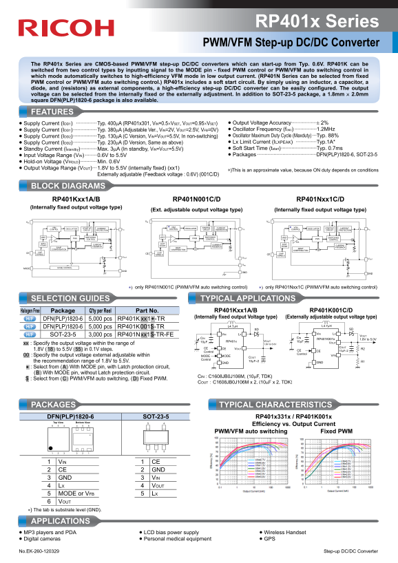
Page 1 Text Content
RP401x Series PWM/VFM Step-up DC/DC Converter
The RP401x Series are CMOS-based PWM/VFM step-up DC/DC converters which can start-up from Typ. 0.6V. RP401K can be switched from two control types by inputting signal to the MODE pin - fixed PWM control or PWM/VFM auto switching control in which mode automatically switches to high-efficiency VFM mode in low output current. (RP401N Series can be selected from fixed PWM control or PWM/VFM auto switching control.) RP401x includes a soft start circuit. By simply using an inductor, a capacitor, a diode, and (resistors) as external components, a high-efficiency step-up DC/DC converter can be easily configured. The output voltage can be selected from the internally fixed or the externally adjustment. In addition to SOT-23-5 package, a 1.8mm × 2.0mm square DFN(PLP)1820-6 package is also available.
FEATURES
• Supply Current (IDD1) ·············· Typ. 400μA (RP401x301, VIN=0.5×VSET, VOUT=0.95×VSET) • Output Voltage Accuracy·················± 2% • Supply Current (IDD1)················ Typ. 380μA (Adjustable Ver., VIN=2V, VOUT=2.5V, VFB=0V) • Oscillator Frequency (fosc) ···············1.2MHz • Supply Current (IDD2)················ Typ. 130μA (C Version, VIN=VOUT=5.5V, In non-switching) • Oscillator Maximum Duty Cycle (Maxduty) ···Typ. 88% • Supply Current (IDD2)················ Typ. 230μA (D Version, Same as above) • Lx Limit Current (ILXPEAK) ··············Typ.1A* • Standby Current (Istandby)···········Max. 3μA (In standby, VIN=VOUT=5.5V) • Soft Start Time (tstart)························Typ. 0.7ms • Input Voltage Range (VIN) ········ 0.6V to 5.5V • Packages ········································DFN(PLP)1820-6, SOT-23-5
• Hold-on Voltage (VHOLD)···········Min. 0.6V • Output Voltage Range (VOUT)··· 1.8V to 5.5V (internally fixed) (xx1)
∗)This is an approximate value, because ON duty depends on conditions
Externally adjustable (Feedback voltage : 0.6V) (001C/D)
BLOCK DIAGRAMS RP401Kxx1A/B RP401N001C/D RP401Nxx1C/D (Internally fixed output voltage type)
(Ext. adjustable output voltage type) (Internally fixed output voltage type)
VIN VIN VIN
VFM STARTUP CURRENT VFM OSCILLATOR STARTUP CURRENT VFM STARTUP CURRENT
CONTROL OSCILLATOR CIRCUIT LX CONTROL CIRCUIT PROTECTION LX CONTROL OSCILLATOR CIRCUIT LX
PROTECTION PROTECTION
VREF PWM SWITCHING VREF PWM SWITCHING VREF SWITCHING
CONTROL CONTROL PWM CONTROL
SOFT CURRENT SOFT CURRENT SOFT START FEEDBACK START FEEDBACK START CURRENT
RAMP RAMP RAMP FEEDBACK
COMPENSATION COMPENSATION COMPENSATION
CE CHIP CHIP
ENABLE CE ENABLE CE CHIP ENABLE
VOUT VOUT
MODE MODE CONTROL
GND GND
∗) only RP401N001C (PWM/VFM auto switching control) ∗) only RP401Nxx1C (PWM/VFM auto switching control)
SELECTION GUIDES TYPICAL APPLICATIONS
Halogen Free Package Q'ty per Reel Part No. RP401Kxx1A/B RP401K001C/D
(Internally fixed output Voltage type) (Externally adjustable output voltage type)
DFN(PLP)1820-6 5,000 pcs RP401K .xx.1.∗ -TR
DFN(PLP)1820-6 5,000 pcs RP401K 001$ -TR SD SD
VIN LX VIN LX
SOT-23-5 3,000 pcs RP401N xx1.$-TR-FE VOUT
CIN CIN
1.8V to 5.0VRP401K001x
10μF RP401x VOUT 10μF
.xx. : Specify the output voltage within the range of 1.8V to 5.0V VOUT CE COUT
1.8V (.18.) to 5.5V (.55.) in 0.1V steps. CE VOUT R2
Control CE CE 10μF×2 Control
.00. : Specify the output voltage external adjustable within MODEMODE VFB
Control
the recommendation range of 1.8V to 5.5V. 10μF×2 GND R1
.∗ : Select from (.A.) With MODE pin, with Latch protection circuit,
(.B.) With MODE pin, without Latch protection circuit.
CIN : C1608JB0J106M, (10μF, TDK)
.$ : Select from (.C.) PWM/VFM auto switching, (.D.) Fixed PWM.
COUT:C1608JB0J106M x 2, (10μF x 2, TDK)
PACKAGES TYPICAL CHARACTERISTICS DFN(PLP)1820-6 SOT-23-5 RP401x331x / RP401K001x
6 5 4 4 5 6 Efficiency vs. Output Current Top View Bottom View
PWM/VFM auto switching Fixed PWM
1 VIN 1 CE 2 CE 2 GND 3 GND 3 VIN 4 LX 4 VOUT 5 MODE or VFB 5 LX 6 VOUT ∗) The tab is substrate level (GND).
APPLICATIONS • MP3 players and PDA • LCD bias power supply • Wireless Handset • Digital cameras • Personal medical equipment • GPS No.EK-260-120329 Step-up DC/DC Converter
Page Summary Contents For RICOH RP401x Series PWM VFM Step-up DC DC Converter Data Sheet User Manual
Manual Details
| Brand | Ricoh |
|---|---|
| Pages | 2 |
| File Size | 329.74 KB |
| Published | June 01, 2026 |
Enter the captcha to get the download link:

Frequently Asked Questions
What input voltage range does the RP401x series support?
The input voltage (VIN) range is 0.6V to 5.5V.
How can I adjust the output voltage?
The output voltage can be selected from internally fixed settings or externally adjusted using the MODE pin and feedback resistors (R2).
What does VFM mode provide when transitioning between control options?
PWM/VFM auto switching automatically switches to high-efficiency VFM mode when operating at low output current.
Which form factors are available for this converter?
It is available in SOT-23-5 and DFN(PLP)1820-6 packages.