# A B C D E F G H I J K L M N O P Q R S T U V W X Y Z

RICOH RN5RK SERIES VFM STEP-UP DC DC CONVERTER User Guide and Data Sheet

Summary

The RN5RK series offers advanced VFM (Chopper) Step-up DC/DC converter ICs designed for efficient power solutions in portable electronics. These CMOS-based converters provide ultra-low supply current and high output voltage accuracy using minimal external components (inductor, diode, capacitor). The manual serves as a comprehensive guide, detailing pin configurations, electrical characteristics, applications—such as battery-powered cameras and communication equipment—and providing selection guidance for varying output voltages and driver options. Ideal for engineers developing energy-efficient power sources requiring stable DC/DC conversion across various demanding applications.
📄 Preview PAGE OF 23

Page 1 Text Content

RN5RK SERIES

VFM STEP-UP DC/DC CONVERTER

NO.EA-045-111124

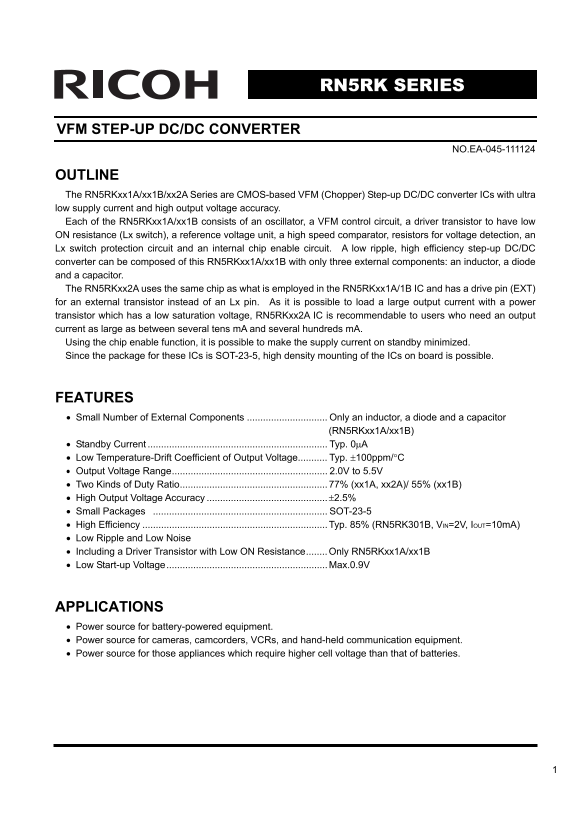
OUTLINE The RN5RKxx1A/xx1B/xx2A Series are CMOS-based VFM (Chopper) Step-up DC/DC converter ICs with ultra low supply current and high output voltage accuracy. Each of the RN5RKxx1A/xx1B consists of an oscillator, a VFM control circuit, a driver transistor to have low ON resistance (Lx switch), a reference voltage unit, a high speed comparator, resistors for voltage detection, an Lx switch protection circuit and an internal chip enable circuit. A low ripple, high efficiency step-up DC/DC converter can be composed of this RN5RKxx1A/xx1B with only three external components: an inductor, a diode and a capacitor. The RN5RKxx2A uses the same chip as what is employed in the RN5RKxx1A/1B IC and has a drive pin (EXT) for an external transistor instead of an Lx pin. As it is possible to load a large output current with a power transistor which has a low saturation voltage, RN5RKxx2A IC is recommendable to users who need an output current as large as between several tens m A and several hundreds m A. Using the chip enable function, it is possible to make the supply current on standby minimized. Since the package for these ICs is SOT-23-5, high density mounting of the ICs on board is possible.

FEATURES • Small Number of External Components Only an inductor, a diode and a capacitor

(RN5RKxx1A/xx1B)

• Standby Current Typ. 0μA • Low Temperature-Drift Coefficient of Output Voltage........... Typ. ±100ppm/°C • Output Voltage Range.......................................................... 2.0V to 5.5V • Two Kinds of Duty Ratio....................................................... 77% (xx1A, xx2A)/ 55% (xx1B) • High Output Voltage Accuracy .............................................±2.5% • Small Packages ................................................................. SOT-23-5 • High Efficiency Typ. 85% (RN5RK301B, VIN=2V, IOUT=10m A) • Low Ripple and Low Noise • Including a Driver Transistor with Low ON Resistance........Only RN5RKxx1A/xx1B • Low Start-up Voltage............................................................Max.0.9V

APPLICATIONS • Power source for battery-powered equipment. • Power source for cameras, camcorders, VCRs, and hand-held communication equipment. • Power source for those appliances which require higher cell voltage than that of batteries.

Page Summary Contents For RICOH RN5RK SERIES VFM STEP-UP DC DC CONVERTER User Guide and Data Sheet

Page 1 RN5RK SERIES VFM STEP-UP DC/DC CONVERTER NO.EA-045-111124 OUTLINE The RN5RKxx1A/xx1B/xx2A Series are CMOS-based VFM (Chopper) Step-up DC/DC converter ICs with ultra low supply current and high output ...
Page 2 RN5RK OUTLINE DIAGRAM RN5RKxx1x RN5RKxx2A Vref Vref Lx 5 VLX limiter VOUT2 EXT VOUT2 Buffer Buffer Lx SW VFM Control VFM Control OSC 100k Hz OSC 100k Hz Error Amp. Error Amp. Chip Enable Chip Enable G...
Page 3 RN5RK PIN CONFIGURATIONS • SOT-23-5 (mark side) PIN DISCRIPTION • RN5RKxx1x • RN5RKxx2A Pin No. Symbol Description Pin No. Symbol Description 1 CE Chip Enable Pin 1 CE Chip Enable Pin 2 VOUT Step-up O...
Page 4 RN5RK ABSOLUTE MAXIMUM RATINGS • RN5RKxx1x Symbol Item Rating Unit VOUT Step-up Output Pin Voltage –0.3 to 9.0 V VLX Lx Pin Voltage –0.3 to 9.0 V VCE CE Pin Voltage –0.3 to VOUT+0.3 V ILX Lx Pin Outpu...
Page 5 RN5RK ELECTRICAL CHARACTERISTICS • RN5RKxx1A/xx1B Topt=25°C Symbol Item Conditions Min. Typ. Max. Unit VOUT Output Voltage VIN=Set VOUT×0.6, IOUT=1m A ×0.975 ×1.025 VIN Input Voltage 8.0 V ΔVOUT/ Outp...
Page 6 RN5RK Symbol Item Conditions Min. Typ. Max. Unit 2.0V Set VOUT 2.4V, VLX=0.4V 2.5V Set VOUT 2.9V, VLX=0.4V 3.0V Set VOUT 3.4V, VLX=0.4V ILX Lx Switching Current 3.5V Set VOUT 3.9V, VLX=0.4V m A 4.0V S...
Page 7 RN5RK • RN5RKxx2A Topt=25°C Symbol Item Conditions Min. Typ. Max. Unit VOUT=VCE=0V→6V, VOUT Output Voltage Judgment is made by the EXT ×0.975 ×1.025 waveform VIN Input Voltage 8.0 V ΔVOUT/ Output Volt...
Page 8 RN5RK TYPICAL APPLICATIONS AND TECHNICAL NOTES RN5RKxx1x RN5RKxx2A LX VOUT Tr EXT VOUT VIN Cb CL1VIN CL2 GND CE GND CE L : 100μH (Sumida, CD54) L : 27μH (Sumida, CD105) SD : MA721 (Matsushita Electron...
Page 9 RN5RK TEST CIRCUITS Lx VOUT Lx VOUT GND CE GND CE CL Test Circuit 1 Test Circuit 2 Lx VOUT GND CE Oscilloscope Test Circuit 3 *)When VLXlim and ILX are measured, the 5Ω resistor is used. Otherwise 1kΩ...
Page 10 RN5RK EXT VOUT EXT VOUT GND CE GND CE CL Test Circuit 1 Test Circuit 2 EXT VOUT EXT VOUT Oscilloscope GND CE GND CE CL Oscilloscope Test Circuit 3 Test Circuit 4 Components Inductor (L) : 27μH (Sumida...
Page 11 RN5RK ut pu t V ol ta ge (V ut pu t V ol ta ge (V ut pu t V ol ta ge (V TYPICAL CHARACTERISTICS • RN5RKxx1A/B 1) Output Voltage vs. Output Current (Topt=25°C) RN5RK301A RN5RK301A 1.3VVIN=0.9V 1.5 VIN=...
Page 12 ffi ci en cy ffi ci en cy ut pu t V ol ta ge (V RN5RK RN5RK501B RN5RK501B VIN=1.5V VIN=1.5V Output Current IOUT(m A) Output Current IOUT(m A) 2) Efficiency vs. Output Current (Topt=25°C) ffi ci en cy ...
Page 13 RN5RK ip pl ol ta ge r( p- p) ffi ci en cy ffi ci en cy RN5RK501A RN5RK501A VIN=0.9V VIN=0.9V Output Current IOUT(m A) Output Current IOUT(m A) RN5RK501B RN5RK501B ip pl ol ta ge r( L=100μH p- p) ffi ...
Page 14 ip pl ol ta ge r( p- p) ip pl ol ta ge r( p- p) ip pl ol ta ge r( p- p) RN5RK RN5RK301B RN5RK301B VIN=1.0V Output Current IOUT(m A) Output Current IOUT(m A) RN5RK501A RN5RK501A ip pl ol ta ge r( p- p)...
Page 15 ta rt -u p/ ol d- on ol ta ge RN5RK ta rt -u p/ ol d- on ol ta ge ut pu t V ol ta ge (V st ar t/V ho ld (V st ar t/V ho ld (V 4) Start-up/Hold-on Voltage vs. Output Current (Topt=25 °C) RN5RK301A RN5R...
Page 16 Lx itc hi ng ur re nt IL x( ol d- on ol ta ge ho ld (V ta rt -u ol ta ge st ar t( RN5RK 6) Start-up Voltage vs. Temperature RN5RK501A RN5RK501B Temperature Topt( ) Temperature Topt( ) Lx itc hi ng ur ...
Page 17 RN5RK sc ul la to ut yc le ax du ty up pl ur re nt ID 2( μA up pl ur re nt ID 1( μA 9) Supply Current 1 vs. Temperature RN5RK301A RN5RK501A Temperature Topt( ) Temperature Topt( ) 10) Supply Current 2...
Page 18 ax im um sc ill at or re qu en cy f O (k z) In pu t V ol ta ge (V RN5RK 13) CE “H” Input Voltage vs. Temperature 14) CE “L” Input Voltage vs. Temperature RN5RK301A RN5RK301A Temperature Topt( ) Temper...
Page 19 RN5RK ip pl ol ta ge r( p- p) ffi ci en cy ut pu t V ol ta ge (V • RN5RKxx2A 1) Output Voltage vs. Output Current (Topt=25°C) RN5RK302A RN5RK502A VIN=1.0V 3.0 1.3VVIN=0.9V Output Current IOUT(m A) Out...
Page 20 ta rt -u p/ ol d- on ol ta ge ut pu t C ur re nt IE (m ut pu t V ol ta ge (V RN5RK st ar t/V ho ld (V 4) Start-up/Hold-on Voltage vs. Output Current (Topt=25°C) RN5RK302A RN5RK502A 1.6 1.2 Vstart,Vhol...
Page 21 RN5RK up pl ur re nt ID 2( μA up pl ur re nt ID 1( μA ut pu t C ur re nt IE L( 7) EXT “L” Output Current vs. Temperature RN5RK302A RN5RK502A Temperature Topt( ) Temperature Topt( ) 8) Supply Current 1...
Page 22 In pu t V ol ta ge (V sc ul la to ut yc le ax du ty RN5RK 11) Oscillator Duty Cycle vs. Temperature 12) Maximum Oscillator Frequency vs. Temperature RN5RK302A RN5RK302A Temperature Topt( ) Temperature...
Page 23 1. The products and the product specifications described in this document are subject to change or discontinuation of production without notice for reasons such as improvement. Therefore, before decid...

Manual Details

Brand Ricoh
Pages 23
File Size 354.13 KB
Published May 31, 2026
67 views

Enter the captcha to get the download link:

captcha

Frequently Asked Questions

What external components are needed to build a step-up converter with this IC?

It requires only three external components: an inductor, a diode, and a capacitor.

Which RN5RK series should I use for large output currents?

The RN5RKxx2A is recommended for output currents between tens mA and several hundred mA because it uses an external drive pin (EXT).

What is the typical standby current draw?

The standby current is typically 0μA, which can be minimized using the chip enable function.

What is the supported output voltage range?

The converter supports a wide output voltage range from 2.0V to 5.5V.