RICOH R1201x SERIES STEP-UP DC DC CONVERTER FOR WHITE LED BACK LIGHT Data Sheet
Summary
The R1201x Series is a highly efficient PWM control step-up DC/DC converter specifically designed for driving white LEDs used in backlight applications. This IC provides constant current capability and multiple protection features (UVLO, OVP). The detailed manual covers the device's operation, including flexible LED dimming control via the CE pin and handling varied input voltages (1.8V to 5.5V). It is ideal for electronics engineers designing high-performance, reliable white LED lighting solutions for portable equipment.
Page 1 Text Content
R1201x SERIES
STEP-UP DC/DC CONVERTER FOR WHITE LED BACK LIGHT
NO.EA-207-120404
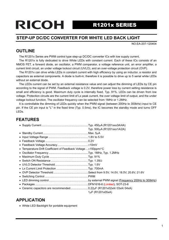
OUTLINE The R1201x Series are PWM control type step-up DC/DC converter ICs with low supply current. The R1201x is fully dedicated to drive White LEDs with constant current. Each of these ICs consists of an NMOS FET, a forward diode, an oscillator, a PWM comparator, a voltage reference unit, an error amplifier, a current limit circuit, an under voltage lockout circuit (UVLO), and an over-voltage protection circuit (OVP). The R1201x can drive white LEDs in constant current with high efficiency by using an inductor, a resistor and capacitors as external components. A diode is built-in; therefore it is possible to drive up to 5 serial white LEDs without an external diode. The LEDs current can be set by an external resistance value and can adjust the dimming of LEDs by CE pin according to the signal of PWM. Feedback voltage is 0.2V, therefore power loss by current setting resistance is small and efficiency is good. Maximum duty cycle is internally fixed, Typ. 91%. LEDs can be driven from low voltage. Protection circuits are the current limit of Lx peak current, the over voltage limit of output, and the under voltage lockout function. The oscillator frequency can be selected from 1MHz or 1.2MHz. It is controllable the dimming of LEDs quickly when the PWM signal (between 200Hz to 300k Hz) input to CE pin. If the CE pin input is "L" in the fixed time (Typ. 0.5ms), the IC becomes the standby mode and turns OFF LEDs.
FEATURES • Supply Current ...........................................................Typ. 450μA (R1201xxx3A/4A)
Typ. 500μA (R1201xxx1A/2A)
• Standby Current .........................................................Max. 5μA • Input Voltage Range ..................................................1.8V to 5.5V • Feedback Voltage ......................................................0.2V • Feedback Voltage Accuracy.......................................±10m V • Temperature-Drift Coefficient of Feedback Voltage ...±150ppm/°C • Oscillator Frequency ..................................................Typ. 1MHz, Typ. 1.2MHz • Maximum Duty Cycle .................................................Typ. 91% • Switch ON Resistance ...............................................Typ. 1.35Ω • UVLO Detector Threshold..........................................Typ. 1.6V • Lx Current Limit Protection ........................................Typ. 700m A • OVP Detector Threshold............................................Select from 9.5V, 14.0V, 18.5V, 20.6V, 21.6V • Switching Control .......................................................PWM • LED dimming control..................................................by external PWM signal (Frequency 200Hz to 300k Hz) • Packages ...................................................................DFN1616-6 (Limited), SOT-23-6 • Ceramic capacitors are recommended......................0.22μF (R1201x02x A/ 03x A/ 04x A) 1μF (R1201x05x A)
APPLICATION • White LED Backlight for portable equipment
Page Summary Contents For RICOH R1201x SERIES STEP-UP DC DC CONVERTER FOR WHITE LED BACK LIGHT Data Sheet
Manual Details
| Brand | Ricoh |
|---|---|
| Pages | 17 |
| File Size | 365.98 KB |
| Published | June 01, 2026 |
Enter the captcha to get the download link:
