# A B C D E F G H I J K L M N O P Q R S T U V W X Y Z

RICOH R3134x SERIES User's Guide and Manual

Summary

This advanced CMOS voltage detector IC is an ideal component for generating reliable system reset signals in low-voltage, critical applications like CPU resets and battery monitoring. The R3134x series offers fixed, highly accurate thresholds and integrates a built-in delay circuit (approx. 240ms) for predictable power sequencing. This documentation serves as an essential guide for embedded engineers, providing detailed block diagrams, selection criteria, pin configurations, and application details necessary to integrate the robust detector into complex hardware designs.
📄 Preview PAGE OF 23

Page 1 Text Content

R3134x SERIES

LOW VOLTAGE DETECTOR WITH BUILT-IN DELAY CIRCUIT

NO.EA-209-120404

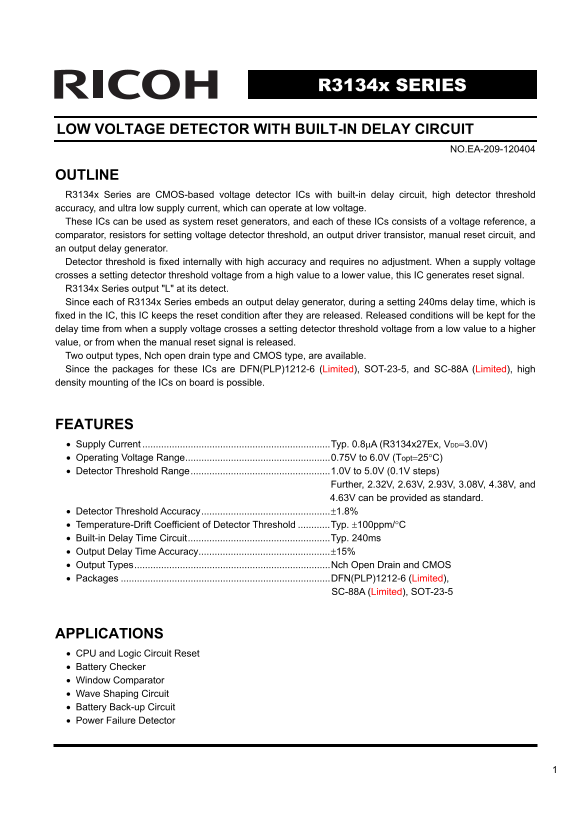
OUTLINE R3134x Series are CMOS-based voltage detector ICs with built-in delay circuit, high detector threshold accuracy, and ultra low supply current, which can operate at low voltage. These ICs can be used as system reset generators, and each of these ICs consists of a voltage reference, a comparator, resistors for setting voltage detector threshold, an output driver transistor, manual reset circuit, and an output delay generator. Detector threshold is fixed internally with high accuracy and requires no adjustment. When a supply voltage crosses a setting detector threshold voltage from a high value to a lower value, this IC generates reset signal. R3134x Series output "L" at its detect. Since each of R3134x Series embeds an output delay generator, during a setting 240ms delay time, which is fixed in the IC, this IC keeps the reset condition after they are released. Released conditions will be kept for the delay time from when a supply voltage crosses a setting detector threshold voltage from a low value to a higher value, or from when the manual reset signal is released. Two output types, Nch open drain type and CMOS type, are available. Since the packages for these ICs are DFN(PLP)1212-6 (Limited), SOT-23-5, and SC-88A (Limited), high density mounting of the ICs on board is possible.

FEATURES • Supply Current ......................................................................Typ. 0.8μA (R3134x27Ex, VDD=3.0V) • Operating Voltage Range......................................................0.75V to 6.0V (Topt=25°C) • Detector Threshold Range....................................................1.0V to 5.0V (0.1V steps)

Further, 2.32V, 2.63V, 2.93V, 3.08V, 4.38V, and 4.63V can be provided as standard.

• Detector Threshold Accuracy................................................±1.8% • Temperature-Drift Coefficient of Detector Threshold ............Typ. ±100ppm/°C • Built-in Delay Time Circuit.....................................................Typ. 240ms • Output Delay Time Accuracy.................................................±15% • Output Types.........................................................................Nch Open Drain and CMOS • Packages ..............................................................................DFN(PLP)1212-6 (Limited),

SC-88A (Limited), SOT-23-5

APPLICATIONS • CPU and Logic Circuit Reset • Battery Checker • Window Comparator • Wave Shaping Circuit • Battery Back-up Circuit • Power Failure Detector

Page Summary Contents For RICOH R3134x SERIES User's Guide and Manual

Page 1 R3134x SERIES LOW VOLTAGE DETECTOR WITH BUILT-IN DELAY CIRCUIT NO.EA-209-120404 OUTLINE R3134x Series are CMOS-based voltage detector ICs with built-in delay circuit, high detector threshold accuracy,...
Page 2 BLOCK DIAGRAMS Nch Open Drain Output (R3134xxx EA) CMOS Output (R3134xxx EC) VDD MR VDD MR Delay DOUT Delay Circuit Circuit GND GND SELECTION GUIDE The package type, the detector threshold, the output...
Page 3 PIN CONFIGURATIONS • DFN(PLP)1212-6 Top View Bottom View • SC-88A • SOT-23-5 5 4 (mark side) (mark side) PIN DESCRIPTIONS • DFN(PLP)1212-6 (Limited) • SC-88A (Limited) Pin No. Symbol Description Pin N...
Page 4 ABSOLUTE MAXIMUM RATINGS Symbol Item Rating Unit VDD Supply Voltage 6.5 V Output Voltage (Nch Open Drain Output) VSS−0.3 to 6.5 Output Voltage (CMOS Output) VSS−0.3 to VDD+0.3 VMR Input Voltage VSS−0....
Page 5 ELECTRICAL CHARACTERISTICS • R3134x The specification in is checked and guaranteed by design engineering at −40°C ≤ Topt ≤ 85°C. Topt=25°C Symbol Item Conditions Min. Typ. Max. Unit VDET Detector Thre...
Page 6 • "H" Output Voltage (VOH) table Topt=25°C "H" Output Voltage VOH (V) Products Detector Threshold VDET (V) Conditions Min. Typ. Max. VDET < 1.2V VDD=VDET+0.1V, IOH=50μA 1.2V ≤ V...
Page 7 DETECTOR THRESHOLD SPECIFICATIONS BY PART NUMBER • R3134x Operating Voltage Detector Threshold Supply Current 1 Part Number VDD [V] VDET [V] ISS1 [μA] Conditions Min. Conditions Min. Min. Typ. Max. Co...
Page 8 Supply Current 2 Supply Current 3 "H" Output Voltage ISS2 [μA] ISS3 [μA] VOH [V] Conditions Typ. Max. Conditions Typ. Max. Conditions Min. VDD=VDET+0.1V IOH=500μA VDD=VDET+0.1V 0.8× IOUT=0A ...
Page 9 MR pin "L" Input "L" Output Voltage MR pin "H" Input Voltage Voltage MR pin pull-up resistance Part Number VOL [V] VIH [V] VIL [V] RMR [MΩ] Conditions Max. Conditions Min...
Page 10 Output Delay Time for Release Detector Threshold Temperature Coefficient tdelay [ms] ΔVDET/ΔTopt [ppm/°C] Conditions Min. Typ. Max. Conditions Typ. VDD=0.8V→ VDET+1.0V 204 240 276 −40°C ≤ Topt ≤ 85°C ...
Page 11 TIMING CHART Detector Threshold Power Supply Minimum (VDD) Operating Voltage Manual Reset (VMR) Output Voltage (VOUT) tdelay tdelay R3134x Operating Diagram DEFINITION OF OUTPUT DELAY TIME Output Dela...
Page 12 OPERATION • Operation of R3134xxx EA Comparator DOUT pin should be pulled-up to an external voltage level. Delay Circuit Vref Rb Nch Block Diagram Detector Threshold VDET =Released Voltage Supply Volt...
Page 13 • Operation of R3134xxx EC Comparator Delay Circuit Vref Rb Nch Block Diagram Detector Threshold VDET =Released Voltage Supply Voltage (VDD) Minimum Operating VDDL Voltage Detect Output Output Voltage...
Page 14 Detector Operation vs. glitch input voltage to the VDD pin Pu ls id th ur in un de r V ET (μ s) When the IC is released and a large pulse (glitch) crosses the detector threshold is forced, the IC may ...
Page 15 TEST CIRCUITS ISS VIN Series DOUT VIN Series Supply Current Test Circuit Detector Threshold Test Circuit (Pull-up circuit is not necessary for CMOS Output type.) VDD VDD R3134x R3134x Series DOUT Seri...
Page 16 VIN Series DOUT Off Leakage Current Test Circuit VDET+1.0V Input Voltage GND VIN R3134x Series DOUT Output Voltage tdelay Output Delay Time Test Circuit (Pull-up circuit is not necessary for CMOS Outp...
Page 17 et ec to r T hr es ho ld T( up pl ur re nt IS (μ up pl ur re nt IS (μ TYPICAL CHARACTERISTICS 1) Supply Current vs. Input Voltage R3134x10Ex R3134x16Ex Topt=85°C Topt=85°C Input Voltage VIN(V) Input V...
Page 18 ri tp rr IO ri tp rr IO et ec to r T hr es ho ld T( R3134x27Ex R3134x48Ex 2.90 5.1 Temperature Topt(°C) Temerature Topt(°C) ri tp rr IO ri tp rr IO et ec to r T hr es ho ld T( 3) Nch Driver Output Cur...
Page 19 ri tp rr IO ri tp rr IO ri tp rr IO 4) Nch Driver Output Current vs. Input Voltage R3134x10Ex R3134x16Ex Topt=85°C Topt=85°C Topt=25°C Topt=25°C Topt=-40°C Topt=-40°C 0.5 1.51.0 0.5 2.01.51.0 Input Vo...
Page 20 ri tp rr IO ri tp rr IO ri tp rr IO R3134x27EC R3134x48EC VDD=6.0V VDD=5.0V VDD=6.0V VDD=4.0V VDD=5.0V VDD=3.0V VDS (V) VDS (V) ri tp rr IO ri tp rr IO ri tp rr IO 6) Pch Driver Output Current vs. Inp...
Page 21 ow er -o es et el ay im ut pu t D el ay im at et ec tio od ut pu t D el ay im at et ec tio od Td el ay (m s) Tr st (μ s) Tr st (μ s) 7) Output Delay Time at Detection Mode vs. Temperature R3134x10Ex R...
Page 22 ow er -o es et el ay im Td el ay (m s) R3134x27Ex R3134x48Ex Temperature Topt(°C) Temperature Topt(°C) ow er -o es et el ay im Td el ay (m s) TECHNICAL NOTES The connection such as Figure A and Figure...
Page 23 1. The products and the product specifications described in this document are subject to change or discontinuation of production without notice for reasons such as improvement. Therefore, before decid...

Manual Details

Brand Ricoh
Pages 23
File Size 336.10 KB
Published June 05, 2026
58 views

Enter the captcha to get the download link:

captcha

Frequently Asked Questions

What is the specified operating voltage range?

The Operating Voltage Range is 0.75V to 6.0V at Topt=25°C.

How accurate is the internal detector threshold and what levels are available?

The threshold accuracy is ±1.8% and can be designated from 1.0V to 5.0V in 0.1V steps.

What function does the built-in delay circuit serve?

It keeps the reset condition active for a fixed duration, typically 240ms, following detection or manual release.

Are there different output types available for selection?

Yes, two output types are available: Nch Open Drain and CMOS type.