# A B C D E F G H I J K L M N O P Q R S T U V W X Y Z

Motorola MPC2605 Product Preview Integrated Secondary Cache for PowerPC Microprocessors User Guide and Data Sheet

Summary

The MPC2605 is an advanced integrated L2 cache designed for PowerPC microprocessors, offering high-speed data caching up to 1MB with zero wait state performance. This sophisticated single chip features copy-back capability and supports scalable configurations for multiple processors in a shared environment. The technical manual provides comprehensive details, including block diagrams, pin assignments, operational modes (write-through/copy-back), and full electrical specifications. It is essential reading for hardware engineers and system architects designing embedded systems using PowerPC architecture who require high-density cache solutions.
📄 Preview PAGE OF 30

Page 1 Text Content

查询MPC2605供应商

Order this document SEMICONDUCTOR TECHNICAL DATA by MPC2605/D

MPC2605

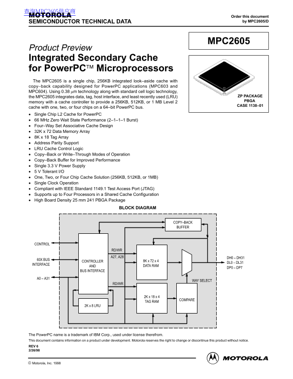
Product Preview Integrated Secondary Cache for Power PC Microprocessors The MPC2605 is a single chip, 256KB integrated look–aside cache with copy–back capability designed for Power PC applications (MPC603 and MPC604). Using 0.38 µm technology along with standard cell logic technology,

the MPC2605 integrates data, tag, host interface, and least recently used (LRU) ZP PACKAGE PBGA

memory with a cache controller to provide a 256KB, 512KB, or 1 MB Level 2

CASE 1138–01

cache with one, two, or four chips on a 64–bit Power PC bus. Single Chip L2 Cache for Power PC 66 MHz Zero Wait State Performance (2–1–1–1 Burst) Four–Way Set Associative Cache Design 32K x 72 Data Memory Array 8K x 18 Tag Array Address Parity Support LRU Cache Control Logic Copy–Back or Write–Through Modes of Operation Copy–Back Buffer for Improved Performance Single 3.3 V Power Supply 5 V Tolerant I/O One, Two, or Four Chip Cache Solution (256KB, 512KB, or 1MB) Single Clock Operation Compliant with IEEE Standard 1149.1 Test Access Port (JTAG) Supports up to Four Processors in a Shared Cache Configuration High Board Density 25 mm 241 PBGA Package

BLOCK DIAGRAM

COPY–BACK BUFFER

CONTROL

RD/WR

A27, A28 DH0 – DH31

60X BUS

CONTROLLER 8K x 72 x 4

DL0 – DL31

INTERFACE

AND DATA RAM

DP0 – DP7

BUS INTERFACE

WAY SELECT

RD/WR

COMPARE

TAG RAM

2K x 8 LRU

The Power PC name is a trademark of IBM Corp., used under license therefrom. This document contains information on a product under development. Motorola reserves the right to change or discontinue this product without notice. REV 6 2/26/98

 Motorola, Inc. 1998 MOTOROLA MPC2605

Page Summary Contents For Motorola MPC2605 Product Preview Integrated Secondary Cache for PowerPC Microprocessors User Guide and Data Sheet

Page 1 查询MPC2605供应商 Order this document SEMICONDUCTOR TECHNICAL DATA by MPC2605/D MPC2605 Product Preview Integrated Secondary Cache for Power PC Microprocessors The MPC2605 is a single chip, 256KB integrat...
Page 2 PIN ASSIGNMENT ABB L2 BG DH20 DH19 DH17 DH31 DH29 DH27 DL16 DL19 DL22DH26 DP6 DL25 DL27 DL29 DL30 CPU3 CFG4 L2 DH23 DH21 DH18 DH16 DH30 DH28 DH25 DL17 DL20 DL23 DL24 DL26 DL28 DL31 DP7 APE BG MISS INH...
Page 3 PIN DESCRIPTIONS Pin Locations Pin Name Type Description 19G, 17H – 19H, 17J – 19J, A0 – A31 I/O Address inputs from processor. Can also be outputs for processor snoop 17K – 19K, 17L – 19L, addresses....
Page 4 Pin Locations Pin Name Type Description 2T CPU4 DBG MPC2605 logically ORs this signal with CPU DBG. Used in multiprocessor configuration as the fourth CPU DBG. 11A – 13A, 15A – 18A, DL0 – DL31 I/O Dat...
Page 5 Pin Locations Pin Name Type Description 2R TRST Test reset input for IEEE 1149.1 boundary scan (JTAG). If JTAG will not be used, TRST should be tied low. 3L TS I/O Transfer start I/O from processor bu...
Page 6 DC OPERATING CONDITIONS AND CHARACTERISTICS (TJ = 20 to + 110°C, Unless Otherwise Noted) RECOMMENDED OPERATING CONDITIONS (Voltages Referenced to VSS = 0 V) Parameter Symbol Min Typ Max Unit Supply Vo...
Page 7 AC OPERATING CONDITIONS AND CHARACTERISTICS (TJ = 20 to + 110°C, Unless Otherwise Noted) Input Timing Measurement Reference Level 1.5 V. . . . . . . . . . . . . . . Output Measurement Timing Level 1.5...
Page 8 AC SPECIFICATIONS MPC2605–66 Timing Reference Min Max Narameter otes Clock Cycle Time ns Input Setup Time 4.5 ns Clock to Input Invalid (Input Hold) ns Clock to Output Driven ns Clock to Output Valid ...
Page 9 MPC2605 RESPONSE TO 60X TRANSFER ATTRIBUTES TT0 – TT4 TBST CI WT Tag Status MPC2605 Response Notes X1X10 Miss Line–fill (processor read miss) 1, 2, 3 X1X10 Hit L2 CLAIM, AACK, TA (processor read hit) ...
Page 10 FUNCTIONAL OPERATION SYSTEM USAGE AND REQUIREMENTS CFG0 – CFG2 These three configuration pins are used to implement the The MPC2605 is a high–performance look–aside cache different cache sizes support...
Page 11 that the processor’s bus grant is negated once there are two If an address tenure is not aborted by an assertion of outstanding data transactions. It is expected that most sys- ARTRY, then the next bu...
Page 12 with the fourth assertion of TA of the first cache read, so that ple ARTRY until two cycles after the assertion of TS, the data the data tenure for the second cache read may commence in read off the b...
Page 13 MEMORY COHERENCE Snoop Kills Kills are snoops that cause cache entries to be immedi- When a processor brings data into its on–chip cache and ately invalidated, regardless of whether they are dirty. Th...
Page 14 The MPC2605 treats multiple processors as one proces- synchronize them internally. This process takes eight clock sor. Thus, the same restrictions on pipelining depth are true cycles. Thus, to guarant...
Page 15 READ HIT/WRITE HIT Figure 1 shows a read hit from an idle bus state. The be a qualified assertion of CPU DBG in the same cycle as the MPC2605 asserts L2 CLAIM the cycle after TS to inform the assertio...
Page 16 MULTIPLE READ/WRITE HITS (NORMAL BUS MODE) Figure 2 is an illustration of MPC2605 pipeline depth limit the data tenure for the first TS is done. The MPC2605 with multiple read hits. The MPC2605 suppor...
Page 17 READ MISS (NORMAL BUS MODE) Figure 3 is an illustration of MPC2605 pipeline depth with a the read miss. This is because the MPC2605 is not in control read miss followed by a read hit. of TA for the fi...
Page 18 MULTIPLE READ HITS (FAST L2 MODE) Back to back pipelined burst read hits for the MPC604 in is a requirement for data streaming. Note also that DBB is Fast L2 mode, also called data streaming mode, are...
Page 19 WRITE THROUGH BURST WRITE HIT Figure 5 shows the fastest possible burst write hit to a the processor when it asserts TS. write–through mode L2 cache line, read miss or write miss The speed at which a ...
Page 20 READ/WRITE MISS Figure 6 is an illustration of a processor read or write miss copyback operation occurs after the processor request is that causes the MPC2605 to replace a dirty line. L2 BR is satisfi...
Page 21 READ/WRITE SNOOP HIT (DIRTY L2 LINE) Figure 7 is an illustration of a read or write snoop to a the processor’s BR signal the cycle following the ARTRY cache line that is dirty in the L2, but is not di...
Page 22 READ/WRITE SNOOP HIT (DIRTY L2 AND PROCESSOR LINE) An illustration of Power PC read or write snoop hit to a dirty the MPC2605 will negate L2 BR. It will also ignore assertions L2 cache line is shown i...
Page 23 READ HIT/WRITE HIT (WITHOUT CPU DBG PARKED) Most of the previous examples have assumed CPU DBG the response for a read hit from the MPC2605 is gated by the is asserted in the same cycle that the proce...
Page 24 AC OPERATING CONDITIONS AND CHARACTERISTICS FOR THE TEST ACCESS PORT (IEEE 1149.1) (TJ = 20 to + 110°C, Unless Otherwise Noted) Input Timing Measurement Reference Level 1.5 V. . . . . . . . . . . . . ...
Page 25 TEST ACCESS PORT DESCRIPTION INSTRUCTION SET pins. The EXTEST instruction would then be loaded. During EXTEST, the boundary–scan register is placed between TDI A five pin IEEE Standard 1149.1 Test Por...
Page 26 TEST–LOGIC RESET RUN–TEST/ SELECT DR–SCAN SELECT IR–SCAN CAPTURE–DR CAPTURE–IR SHIFT–DR SHIFT–IR EXIT1–DR EXIT1–IR PAUSE 1–DR PAUSE–IR EXIT2–DR EXIT2–IR UPDATE–DR UPDATE–IR NOTE: The value adjacent to...
Page 27 BOUNDARY SCAN ORDER BIT NUMBER Bit Bit/Pin Output Number Bit/Pin Name Type Enable The order of the boundary scan chain. Bit 0 is the closest to TDO. DH28 I/O DOE BIT/PIN NAME DH29 I/O DOE The name of ...
Page 28 Bit Bit/Pin Output Bit Bit/Pin Output Number Bit/Pin Name Type Enable Number Bit/Pin Name Type Enable TT1 I/O AOE DL10 I/O DOE TT2 I/O AOE DL11 I/O DOE TT4 I/O AOE DL12 I/O DOE TT3 I/O AOE DL13 I/O DO...
Page 29 Bit Bit/Pin Output Bit Bit/Pin Output Number Bit/Pin Name Type Enable Number Bit/Pin Name Type Enable CFG3 Input FDNOE Output Enable L2 CI Input DBBOE Output L2 FLUSH Input Enable AP0 I/O AOE DOE Outp...
Page 30 PACKAGE DIMENSIONS ZP PACKAGE PBGA CASE 1138–01 NOTES: E2 1. DIMENSIONING AND TOLERANCING PER ASME Y14.5M, 1994. 2. DIMENSIONS IN MILLIMETERS. 3. DIMENSION b IS THE SOLDER BALL DIAMETER MEASURED PARAL...

Manual Details

Brand Motorola
Pages 30
File Size 295.88 KB
Published June 05, 2026
55 views

Enter the captcha to get the download link:

captcha

Frequently Asked Questions

What cache sizes can the MPC2605 support?

The device supports three options: 256KB, 512KB, or 1MB Level 2 cache.

How many processors can share this integrated cache?

It supports up to four processors in a shared cache configuration.

What operational modes are available for the cache?

It operates in Copy–Back or Write–Through modes of operation and has dedicated address parity support.

Are there specific usage restrictions for this product?

The product must not be used in systems intended for surgical implant, life support, or other critical applications.