MOTOROLA MUN2111T1 SERIES Data Sheet User Guide
Summary
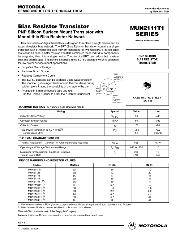
This advanced PNP Silicon Transistor features a monolithic bias resistor network (BRT), integrating multiple components into a single surface mount device. Ideal for simplifying circuit design and minimizing board space in low-power applications. This technical manual provides comprehensive electrical characteristics, maximum ratings, and thermal data for the SC–59 package across various models. It is essential documentation for electronics engineers and designers building compact, reliable circuitry.
Page 1 Text Content
Order this document
SEMICONDUCTOR TECHNICAL DATA by MUN2111T1/D
PNP Silicon Surface Mount Transistor with Monolithic Bias Resistor Network
Motorola Preferred Devices
This new series of digital transistors is designed to replace a single device and its external resistor bias network. The BRT (Bias Resistor Transistor) contains a single transistor with a monolithic bias network consisting of two resistors; a series base resistor and a base–emitter resistor. The BRT eliminates these individual components
by integrating them into a single device. The use of a BRT can reduce both system PNP SILICON cost and board space. The device is housed in the SC–59 package which is designed BIAS RESISTOR for low power surface mount applications. TRANSISTOR
Simplifies Circuit Design Reduces Board Space
Reduces Component Count
COLLECTOR The SC–59 package can be soldered using wave or reflow. (OUTPUT)
The modified gull–winged leads absorb thermal stress during R1 soldering eliminating the possibility of damage to the die.
Available in 8 mm embossed tape and reel
Use the Device Number to order the 7 inch/3000 unit reel. (INPUT)
PIN1 CASE 318D–03, STYLE 1 EMITTER
(SC–59)
(GROUND)
MAXIMUM RATINGS (TA = 25°C unless otherwise noted)
Rating Symbol Value Unit
Collector–Base Voltage VCBO Vdc Collector–Emitter Voltage VCEO Vdc Collector Current IC m Adc Total Power Dissipation @ TA = 25°C(1) PD *200 m W Derate above 25°C 1.6 m W/°C
THERMAL CHARACTERISTICS Thermal Resistance — Junction–to–Ambient (surface mounted) RθJA °C/W Operating and Storage Temperature Range TJ, Tstg –65 to +150 °C Maximum Temperature for Soldering Purposes, TL °C Time in Solder Bath Sec
DEVICE MARKING AND RESISTOR VALUES
Device Marking R1 (K) R2 (K) MUN2111T1 6A MUN2112T1 6B MUN2113T1 6C MUN2114T1 6D MUN2115T1(2) 6E MUN2116T1(2) 6F 4.7 MUN2130T1(2) 6G 1.0 1.0 MUN2131T1(2) 6H 2.2 2.2 MUN2132T1(2) 6J 4.7 4.7 MUN2133T1(2) 6K 4.7 MUN2134T1(2) 6L
1. Device mounted on a FR–4 glass epoxy printed circuit board using the minimum recommended footprint. 2. New devices. Updated curves to follow in subsequent data sheets. Thermal Clad is a trademark of the Bergquist Company Preferred devices are Motorola recommended choices for future use and best overall value.
REV 5
Motor la, Inc. 1996 1Motorola Small–Signal Transistors, FETs and Diodes Device Data
Page Summary Contents For MOTOROLA MUN2111T1 SERIES Data Sheet User Guide
Manual Details
| Brand | Motorola |
|---|---|
| Pages | 10 |
| File Size | 236.97 KB |
| Published | May 29, 2026 |
Enter the captcha to get the download link:

Frequently Asked Questions
What benefit do Bias Resistor Transistors (BRTs) provide compared to separate components?
The BRT integrates the transistor with a monolithic bias network, reducing component count and board space.
How should this device be soldered or mounted on a PCB?
It can be soldered using wave or reflow methods; modified gull–winged leads absorb thermal stress during soldering.
What is the total power dissipation rating at 25°C?
The maximum total power dissipation (Pd) is rated at 200 mW at 25°C.
What is the recommended operating temperature range for the transistor?
The device supports an Operating and Storage Temperature Range of -65 to +150 °C.