MOTOROLA MUN5111DW1T1 SERIES DATA SHEET
Summary
Discover an advanced solution in small-signal electronics: a PNP Silicon Surface Mount Transistor featuring an integrated Bias Resistor Network (BRT). This compact component significantly simplifies circuit design by combining multiple resistors and a transistor into a single package, drastically reducing both board space and overall component count. Technical datasheets provide engineers with comprehensive specifications, including electrical performance characteristics, thermal ratings, and detailed resistor values necessary for designing high-efficiency, low-power surface mount circuits. Ideal for applications prioritizing minimal footprint.
Page 1 Text Content
查询MUN5111DW1T1/D供应商
Order this document
SEMICONDUCTOR TECHNICAL DATA by MUN5111DW1T1/D
PNP Silicon Surface Mount Transistors with
Motorola Preferred Devices
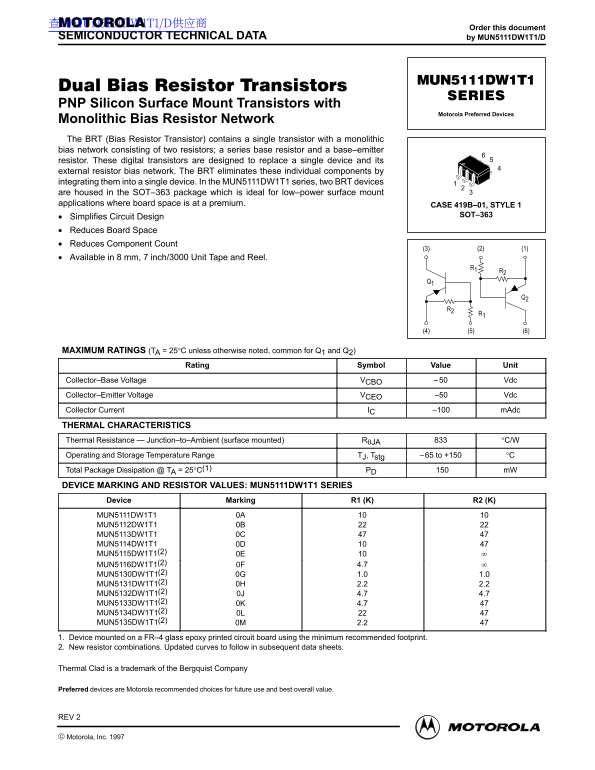
Monolithic Bias Resistor Network The BRT (Bias Resistor Transistor) contains a single transistor with a monolithic bias network consisting of two resistors; a series base resistor and a base–emitter resistor. These digital transistors are designed to replace a single device and its external resistor bias network. The BRT eliminates these individual components by integrating them into a single device. In the MUN5111DW1T1 series, two BRT devices are housed in the SOT–363 package which is ideal for low–power surface mount applications where board space is at a premium. CASE 419B–01, STYLE 1
Simplifies Circuit Design SOT–363
Reduces Board Space Reduces Component Count
Available in 8 mm, 7 inch/3000 Unit Tape and Reel.
MAXIMUM RATINGS (TA = 25°C unless otherwise noted, common for Q1 and Q2)
Rating Symbol Value Unit
Collector–Base Voltage VCBO –50 Vdc Collector–Emitter Voltage VCEO –50 Vdc Collector Current IC –100 m Adc
THERMAL CHARACTERISTICS Thermal Resistance — Junction–to–Ambient (surface mounted) RθJA °C/W Operating and Storage Temperature Range TJ, Tstg –65 to +150 °C Total Package Dissipation @ TA = 25°C(1) PD *150 m W DEVICE MARKING AND RESISTOR VALUES: MUN5111DW1T1 SERIES
Device Marking R1 (K) R2 (K) MUN5111DW1T1 0A MUN5112DW1T1 0B MUN5113DW1T1 0C MUN5114DW1T1 0D MUN5115DW1T1(2) 0E MUN5116DW1T1(2) 0F 4.7 MUN5130DW1T1(2) 0G 1.0 1.0 MUN5131DW1T1(2) 0H 2.2 2.2 MUN5132DW1T1(2) 0J 4.7 4.7 MUN5133DW1T1(2) 0K 4.7 MUN5134DW1T1(2) 0L MUN5135DW1T1(2) 0M 2.2
1. Device mounted on a FR–4 glass epoxy printed circuit board using the minimum recommended footprint. 2. New resistor combinations. Updated curves to follow in subsequent data sheets.
Thermal Clad is a trademark of the Bergquist Company
Preferred devices are Motorola recommended choices for future use and best overall value.
REV 2
Motor la, Inc. 1997 1Motorola Small–Signal Transistors, FETs and Diodes Device Data
Page Summary Contents For MOTOROLA MUN5111DW1T1 SERIES DATA SHEET
Manual Details
| Brand | Motorola |
|---|---|
| Pages | 12 |
| File Size | 218.66 KB |
| Published | June 01, 2026 |
Enter the captcha to get the download link:

Frequently Asked Questions
What is the primary benefit of using a Bias Resistor Transistor (BRT)?
The BRT simplifies circuit design by integrating a monolithic bias network into a single device, eliminating multiple external components.
What package type and form factor are ideal for the MUN5111DW1T1 in?
It uses the SOT–363 package, which is suitable for low-power surface mount applications where board space is limited.
How is the thermal dissipation rated for this device at 25°C?
The total package dissipation is listed at P*150 mW when mounted on an FR-4 glass epoxy printed circuit board.
What does the device marking code indicate about resistor values?
The MUN5111DW1T1 has a specific combination of R1 (K) 0A and R2 (K) 10, while other parts use different codes (e.g., MUN5134DW1T1 is 0L).