# A B C D E F G H I J K L M N O P Q R S T U V W X Y Z

LINEAR TECHNOLOGY LTC1871 1871fc Wide Input Range, No RSENSE Current Mode Boost, Flyback and SEPIC Controller

Summary

The LTC1871 is a high-efficiency current mode controller designed for boosting, SEPIC, and flyback applications in portable electronics. It features an ultra-wide input range of 2.5V to 36V and eliminates the need for sense resistors by utilizing advanced power MOSFET control. This manual provides comprehensive technical details on achieving optimized power management for low to medium power projects, including adjustable frequency control and burst mode operation suitable for battery-powered systems.
📄 Preview PAGE OF 36

Page 1 Text Content

LTC1871 TM

Wide Input Range, No RSENSE

Current Mode Boost, Flyback and SEPIC Controller

FEATURES DESCRIPTIO High Efficiency (No Sense Resistor Required) The LTC®1871 is a wide input range, current mode, boost, Wide Input Voltage Range: 2.5V to 36V flyback or SEPIC controller that drives an N-channel Current Mode Control Provides Excellent power MOSFET and requires very few external compo-

Transient Response nents. Intended for low to medium power applications, it High Maximum Duty Cycle (92% Typ) eliminates the need for a current sense resistor by utiliz- ±2% RUN Pin Threshold with 100m V Hysteresis ing the power MOSFET’s on-resistance, thereby maximiz- ±1% Internal Voltage Reference ing efficiency.

Micropower Shutdown: IQ = 10µA

The IC’s operating frequency can be set with an external

Programmable Operating Frequency

resistor over a 50k Hz to 1MHz range, and can be synchro-

(50k Hz to 1MHz) with One External Resistor

nized to an external clock using the MODE/SYNC pin.

Synchronizable to an External Clock Up to 1.3 × f OSC

Burst Mode operation at light loads, a low minimum

User-Controlled Pulse Skip or Burst Mode® Operation

operating supply voltage of 2.5V and a low shutdown

Internal 5.2V Low Dropout Voltage Regulator

quiescent current of 10µA make the LTC1871 ideally

Output Overvoltage Protection

suited for battery-operated systems.

Capable of Operating with a Sense Resistor for High

Output Voltage Applications For applications requiring constant frequency operation, Small 10-Lead MSOP Package Burst Mode operation can be defeated using the MODE/ SYNC pin. Higher output voltage boost, SEPIC and fly- back applications are possible with the LTC1871 by

EF FI CI EN CY

APPLICATIO S

connecting the SENSE pin to a resistor in the source of the power MOSFET.

Telecom Power Supplies Portable Electronic Equipment The LTC1871 is available in the 10-lead MSOP package.

, LTC and LT are registered trademarks of Linear Technology Corporation. Burst Mode is a registered trademark of Linear Technology Corporation. No RSENSE is a trademark of Linear Technology Corporation. All other trademarks are the property of their respective owners.

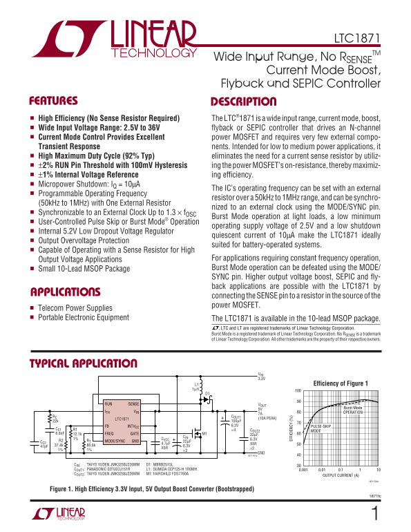
TYPICAL APPLICATIO

VIN 3.3V

L1 Efficiency of Figure 1

RUN SENSE VOUT

Burst Mode

ITH VIN OPERATION

RC COUT1

LTC1871 (10A PEAK)

22k 150µF FB INTVCC 6.3V PULSE-SKIP

CC1 R1 ×4 COUT2

6.8n F 12.1k FREQ GATE M1 22µF

1% CVCC 6.3V

CC2 R2 RT MODE/SYNC GND 22µF

GND 1871 F01a

CIN: TAIYO YUDEN JMK325BJ226MM D1: MBRB2515L COUT1: PANASONIC EEFUEOJ151R L1: SUMIDA CEP125-H 1R0MH 0.001 0.01 0.1 COUT2: TAIYO YUDEN JMK325BJ226MM M1: FAIRCHILD FDS7760A

OUTPUT CURRENT (A)

Figure 1. High Efficiency 3.3V Input, 5V Output Boost Converter (Bootstrapped)

1871fc

Page Summary Contents For LINEAR TECHNOLOGY LTC1871 1871fc Wide Input Range, No RSENSE Current Mode Boost, Flyback and SEPIC Controller

Page 1 LTC1871 TM Wide Input Range, No RSENSE Current Mode Boost, Flyback and SEPIC Controller FEATURES DESCRIPTIO High Efficiency (No Sense Resistor Required) The LTC®1871 is a wide input range, current mod...
Page 2 LTC1871 ABSOLUTE AXI U RATI GS PACKAGE/ORDER I FOR ATIO (Note 1) TOP VIEW VIN Voltage –0.3V to 36V RUN SENSE ITH VIN INTVCC Voltage –0.3V to 7V FB INTVCC INTVCC Output Current 50m A FREQ GATE MODE/ GN...
Page 3 LTC1871 ELECTRICAL CHARACTERISTICS The ● denotes specifications which apply over the full operating temperature range, otherwise specifications are at TA = 25°C. VIN = VINTVCC = 5V, VRUN = 1.5V, RFREQ...
Page 4 SH UT DO OD (µ A) FB OL TA GE (V LTC1871 ELECTRICAL CHARACTERISTICS The ● denotes specifications which apply over the full operating temperature range, otherwise specifications are at TA = 25°C. VIN =...
Page 5 GA TE RE QU EN CY (k Hz RU TH RE SH OL DS (V Bu rs t M od (µ A) LTC1871 TYPICAL PERFOR A CE CHARACTERISTICS Gate Drive Rise and Fall Time Burst Mode IQ vs Temperature vs CLDynamic IQ vs Frequency CL =...
Page 6 IN TV CC OL TA GE (V LTC1871 TYPICAL PERFOR A CE CHARACTERISTICS INTVCC Dropout Voltage INTVCC Load Regulation vs Current, Temperature INTVCC Line Regulation VIN = 7.5V 5.1 IN TV CC OL TA GE (V VIN (V...
Page 7 LTC1871 BLOCK DIAGRA BIAS AND SLOPE START-UP C2 COMPENSATION CONTROL FREQ VIN OSCV-TO-I MODE/SYNC INTVCC PWM LATCH 50k LOGIC BURST CURRENT SENSE COMPARATOR COMPARATOR FB C1 V-TO-I RLOOP INTVCC ILOOP L...
Page 8 LTC1871 OPERATIO Main Control Loop to rise, which causes the current comparator C1 to trip at a higher peak inductor current value. The average inductor The LTC1871 is a constant frequency, current mo...
Page 9 LTC1871 OPERATIO Programming the Operating Mode power MOSFET RDS(ON). If the ITH pin drops below 0.30V, the Burst Mode comparator B1 will turn off the power For applications where maximizing the effic...
Page 10 LTC1871 APPLICATIO S I FOR ATIO When the oscillator’s internal logic circuitry detects a to charge and discharge an internal oscillator capacitor. A synchronizing signal on the MODE/SYNC pin, the inte...
Page 11 LTC1871 APPLICATIO S I FOR ATIO VIN INPUT SUPPLY 2.5V TO 30V R2 R1 5.2V INTVCC CVCC 4.7µF LOGIC DRIVER M1 PLACE AS CLOSE AS POSSIBLE TO DEVICE PINS Figure 7. Bypassing the LDO Regulator and Gate Drive...
Page 12 LTC1871 APPLICATIO S I FOR ATIO caused by the current flowing into the FB pin during The turn-on and turn-off input voltage thresholds are normal operation is less than 1% (this translates to a progra...
Page 13 LTC1871 APPLICATIO S I FOR ATIO Application Circuits The maximum duty cycle, DMAX, should be calculated at minimum VIN. A basic LTC1871 application circuit is shown in Figure 1. External component sel...
Page 14 LTC1871 APPLICATIO S I FOR ATIO Remember that boost converters are not short-circuit Boost Converter: Inductor Core Selection protected. Under a shorted output condition, the inductor Once the value f...
Page 15 LTC1871 AX IM UM UR RE NT EN SE OL TA GE (m V) APPLICATIO S I FOR ATIO a lithium-ion battery or a 3.3V logic supply), then sublogic- Another method of choosing which power MOSFET to use level threshol...
Page 16 LTC1871 APPLICATIO S I FOR ATIO and the RDS(ON) of the MOSFET listed in the manufacturer’s The RTH(JA) to be used in this equation normally includes data sheet. the RTH(JC) for the device plus the the...
Page 17 LTC1871 APPLICATIO S I FOR ATIO For many designs it is possible to choose a single capaci- tested for use in switching power supplies. An excellent tor type that satisfies both the ESR and bulk C requ...
Page 18 LTC1871 APPLICATIO S I FOR ATIO Table 1. Recommended Component Manufacturers VENDOR COMPONENTS TELEPHONE WEB ADDRESS AVX Capacitors (207) 282-5111 avxcorp.com BH Electronics Inductors, Transformers (9...
Page 19 LTC1871 APPLICATIO S I FOR ATIO The output voltage ripple can increase during Burst Mode 1. The supply current into VIN. The VIN current is the sum operation if ∆IL is substantially less than IBURST. ...
Page 20 LTC1871 APPLICATIO S I FOR ATIO resistor value would be 10mΩ, and the power dissi- VIN = 3.3V VOUT = 5V pated in this resistor would be 514m W at maximum MODE/SYNC = INTVCC 2A/DIV (PULSE-SKIP MODE) ou...
Page 21 LTC1871 APPLICATIO S I FOR ATIO The inductor ripple current is: ESR ceramic. Based on a maximum output ripple voltage of 1%, or 50m V, the bulk C needs to be great- =I AL er than: And so the inductor ...
Page 22 LTC1871 APPLICATIO S I FOR ATIO PC Board Layout Checklist source of the power MOSFET or the bottom terminal of the sense resistor, 4) the negative terminal of the input 1. In order to minimize switchi...
Page 23 LTC1871 APPLICATIO S I FOR ATIO 2. Beware of ground loops in multiple layer PC boards. Try pin trace and any high frequency switching nodes. The to maintain one central ground node on the board and LT...
Page 24 LTC1871 APPLICATIO S I FOR ATIO SEPIC Converter Applications buck-boost converter. The two inductors L1 and L2 can be independent but can also be wound on the same core since The LTC1871 is also well ...
Page 25 LTC1871 APPLICATIO S I FOR ATIO The constant ‘χ’ represents the fraction of ripple current in By making L1 = L2 and winding them on the same core, the the inductor relative to its maximum value. For e...
Page 26 LTC1871 APPLICATIO S I FOR ATIO are limited to 30V or less. Check the switching waveforms sensing element, care should be taken to ensure that the directly across the drain and source terminals of the...
Page 27 LTC1871 APPLICATIO S I FOR ATIO and the diode junction temperature is: For many designs it is possible to choose a single capaci- tor type that satisfies both the ESR and bulk C require- TJ = TA + PD ...
Page 28 LTC1871 APPLICATIO S I FOR ATIO choice is AVX TPS series of surface mount tantalum. Also, which is typically close to VIN(MAX). The ripple current ceramic capacitors are now available with extremely l...
Page 29 LTC1871 APPLICATIO S I FOR ATIO And so the inductor value is: SENSE MAX DS ON MIN MAX +⎛ µ( HIN MAX= ⎝⎜ ⎠⎟ ⎝⎜ IN MIN ⎠⎟ The component chosen is a BH Electronics BH510- 1007, which has a saturation cur...
Page 30 LTC1871 APPLICATIO S I FOR ATIO VIN = 4.5V VIN = 15V VOUT = 12V VOUT = 12V VOUT (AC) VOUT (AC) 200m V/DIV 200m V/DIV IOUT IOUT 0.5A/DIV 0.5A/DIV 50µs/DIV 1871 F19a 50µs/DIV 1871 F19b Figure 19. LTC187...
Page 31 LTC1871 TYPICAL APPLICATIO S 2.5V to 3.3V Input, 5V/2A Output Boost Converter VIN 2.5V to 3.3V RUN SENSE VOUT ITH VIN 5V 2A COUT1 RC LTC1871 EF FI CI EN CY 6.3V COUT2 FB INTVCC CC1 R1 10µF 6.8n F 12.1...
Page 32 LTC1871 TYPICAL APPLICATIO S 18V to 27V Input, 28V Output, 400W 2-Phase, Low Ripple, Synchronized RF Base Station Power Supply (Boost) VIN 18V to 27V RUN SENSE D1 ITH VIN LTC1871 47p F COUT1 FB INTVCC...
Page 33 LTC1871 TYPICAL APPLICATIO S 4.5V to 28V Input, 5V/2A Output SEPIC Converter with Undervoltage Lockout and Soft-Start VIN R1 4.5V to 28V 115k CDC 1%R2 2.2µF L1* RUN SENSE ×3 D1 VOUT ITH VIN 2A RC LTC1...
Page 34 LTC1871 TYPICAL APPLICATIO S 5V to 15V Input, –5V/5A Output Positive-to-Negative Converter with Undervoltage Lockout and Level-Shifted Feedback VIN 5V to 15V VOUT –5V 5A RUN SENSE ITH VIN CDC 100µF LT...
Page 35 LTC1871 PACKAGE DESCRIPTIO MS Package 10-Lead Plastic MSOP (Reference LTC DWG # 05-08-1661) (NOTE 3) (.0120 ± .0015) (.0197) (.0196 ± .003) TYP BSC REF RECOMMENDED SOLDER PAD LAYOUT DETAIL “A” (.118 ±...
Page 36 LTC1871 TYPICAL APPLICATIO S High Power SLIC Supply with Undervoltage Lockout (Also See the LTC3704 Data Sheet) D2 C3 10BQ0604 10µF 25V R2 7V TO 12V 49.9k 150k VOUT1 1% 1% –24V CR CIN 1n F 220µF COUT ...

Manual Details

Brand Current
Pages 36
File Size 414.00 KB
Published May 30, 2026
75 views

Enter the captcha to get the download link:

captcha

Frequently Asked Questions

How does the LTC1871 achieve high efficiency without a sense resistor?

It utilizes the power MOSFET’s on-resistance, thereby eliminating the need for an external current sense resistor.

What input voltage range can this controller handle?

The LTC1871 provides a wide input voltage range spanning from 2.5V up to 36V, suitable for flyback or SEPIC topologies.

Can the switching frequency be customized?

Yes, the operating frequency can be controlled using an external resistor, allowing it to operate between 50kHz and 1MHz.

Is this controller safe for battery-operated devices?

It is designed with output overvoltage protection, a low dropout voltage regulator, and micropower shutdown to suit battery applications.