# A B C D E F G H I J K L M N O P Q R S T U V W X Y Z

LINEAR TECHNOLOGY LTC2482 16-Bit ΔΣ ADC with Easy Drive Input Current Cancellation Data Sheet User Manual

Summary

The LTC2482 is a high-precision 16-bit $\Delta\Sigma$ Analog-to-Digital Converter featuring patented Easy Drive Technology for superior signal integrity. This advanced ADC provides robust rail-to-rail input capabilities while automatically canceling common-mode differential current errors, ensuring exceptional accuracy even across wide voltage ranges. The manual details its usage in critical applications such as weight scales, strain measurement, and industrial process control. It is ideal for engineers requiring ultra-low noise (600nV RMS) data acquisition with simultaneous rejection of 50Hz/60Hz line frequency interference.
📄 Preview PAGE OF 32

Page 1 Text Content

LTC2482

16-Bit ∆Σ ADC with Easy Drive Input Current Cancellation

FEATURES DESCRIPTIO

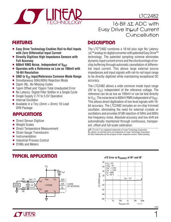
Easy Drive Technology Enables Rail-to-Rail Inputs The LTC®2482 combines a 16-bit plus sign No Latency with Zero Differential Input Current ∆Σ™ analog-to-digital converter with patented Easy Drive™ Directly Digitizes High Impedance Sensors with technology. The patented sampling scheme eliminates Full Accuracy dynamic input current errors and the shortcomings of on- 600n V RMS Noise, Independent of VREF chip buffering through automatic cancellation of differen- Operates with a Reference as Low as 100m V with tial input current. This allows large external source 16-Bit Resolution impedances and input signals with rail-to-rail input range GND to VCC Input/Reference Common Mode Range to be directly digitized while maintaining exceptional DC Simultaneous 50Hz/60Hz Rejection Mode accuracy.

2ppm INL, No Missing Codes

The LTC2482 allows a wide common mode input range

1ppm Offset and 15ppm Total Unadjusted Error

(0V to VCC) independent of the reference voltage. The

No Latency: Digital Filter Settles in a Single Cycle

reference can be as low as 100m V or can be tied directly

Single Supply 2.7V to 5.5V Operation

to VCC. The noise level is 600n V RMS independent of VREF.

+F ER RO (p pm

Internal Oscillator

This allows direct digitization of low level signals with 16-

Available in a Tiny (3mm × 3mm) 10-Lead

bit accuracy. The LTC2482 includes an on-chip trimmed

DFN Package

oscillator, eliminating the need for external crystals or oscillators and provides 87d B rejection of 50Hz and 60Hz

APPLICATIO S

line frequency noise. Absolute accuracy and low drift are

Direct Sensor Digitizer automatically maintained through continuous, transpar- Weight Scales ent, offset and full-scale calibration. Direct Temperature Measurement

, LTC and LT are registered trademarks of Linear Technology Corporation. No Latency ∆Σ and Easy Drive are trademarks of Linear Technology Corporation.

Strain Gauge Transducers

All other trademarks are the property of their respective owners. Patent pending.

Instrumentation Industrial Process Control DVMs and Meters

TYPICAL APPLICATIO

+FS Error vs RSOURCE at IN+ and IN–

VCC = 5V VCC VREF = 5V + = 3.75V VIN – = 1.25V VIN

1µF FO = GND

TA = 25°C

CIN = 1µF

10k IDIFF = 0 VREF VCC

SCK 3-WIRE

SENSE 1µF LTC2482 –20

SPI INTERFACE CS

10k GND FO

2482 TA01

1k 10k 100k RSOURCE (Ω) 2482 TA02

Page Summary Contents For LINEAR TECHNOLOGY LTC2482 16-Bit ΔΣ ADC with Easy Drive Input Current Cancellation Data Sheet User Manual

Page 1 LTC2482 16-Bit ∆Σ ADC with Easy Drive Input Current Cancellation FEATURES DESCRIPTIO Easy Drive Technology Enables Rail-to-Rail Inputs The LTC®2482 combines a 16-bit plus sign No Latency with Zero Dif...
Page 2 LTC2482 ABSOLUTE AXI U RATI GS PACKAGE/ORDER I FOR ATIO (Notes 1, 2) Supply Voltage (VCC) to GND...................... –0.3V to 6V TOP VIEW ORDER PART Analog Input Voltage to GND –0.3V to (VCC + 0.3V)...
Page 3 LTC2482 CO VERTER CHARACTERISTICS The ● denotes specifications which apply over the full operating temperature range, otherwise specifications are at TA = 25°C. (Notes 3, 4) PARAMETER CONDITIONS MIN T...
Page 4 LTC2482 DIGITAL I PUTS A D DIGITAL OUTPUTS The ● denotes specifications which apply over the full operating temperature range, otherwise specifications are at TA = 25°C. (Note 3) SYMBOL PARAMETER COND...
Page 5 LTC2482 TI G CHARACTERISTICS The ● denotes specifications which apply over the full operating temperature range, otherwise specifications are at TA = 25°C. (Note 3) SYMBOL PARAMETER CONDITIONS MIN TYP...
Page 6 TU (p pm EF IN (p pm EF LTC2482 TYPICAL PERFOR A CE CHARACTERISTICS OF FS ET RR OR (p pm EF Integral Nonlinearity Integral Nonlinearity Integral Nonlinearity (VCC = 5V, VREF = 5V) (VCC = 5V, VREF = 2....
Page 7 LTC2482 TYPICAL PERFOR A CE CHARACTERISTICS RE JE CT IO (d B) OF FS ET RR OR (p pm FR EQ UE NC (k Hz EF Offset Error vs VCC Offset Error vs VREF 0.3 0.3 REF+ = 2.5V VCC = 5V REF– = GND REF– = GND 0.2 ...
Page 8 LTC2482 TYPICAL PERFOR A CE CHARACTERISTICS RE JE CT IO (d B) SL EE OD CU RR EN (µ A) Conversion Current PSRR vs Frequency at VCC vs Temperature VCC = 4.1V DC ±0.7V FO = GND VREF = 2.5V CS = GND IN+ =...
Page 9 LTC2482 PI FU CTIO S GND (Pin 1): Ground. This pin should be tied to ground; GND (Pin 8): Ground. Shared pin for analog ground, however, in order to remain pin compatible with the digital ground and r...
Page 10 LTC2482 FU CTIO AL BLOCK DIAGRA VREF VCC IN+ REF+ SERIAL SD0 3RD ORDER ∆Σ ADC INTERFACE IN– CS IN– REF– AUTOCALIBRATION FO AND CONTROL INTERNAL OSCILLATOR 2482 FD TEST CIRCUITS 1.69k CLOAD = 20p F CLO...
Page 11 LTC2482 TI I G DIAGRA S Timing Diagram Using Internal SCK t KQMIN t KQMAX SLEEP CONVERSIONDATA OUT 2482 TD1 Timing Diagram Using External SCK UU WU t5 t KQMIN t6 t KQMAX SCK t4 SLEEP CONVERSIONDATA OU...
Page 12 LTC2482 APPLICATIO S I FOR ATIO While in this sleep state, power consumption is reduced by rent. This enables external RC networks and high imped- two orders of magnitude. The part remains in the slee...
Page 13 LTC2482 APPLICATIO S I FOR ATIO Bit 23 (first output bit) is the end of conversion (EOC) Data is shifted out of the SDO pin under control of the serial indicator. This bit is available at the SDO pin ...
Page 14 LTC2482 APPLICATIO S I FOR ATIO Conversion Clock normal mode rejection in a frequency range of f EOSC/5120 ±4% and its harmonics. The normal mode rejection as a A major advantage the delta-sigma conve...
Page 15 LTC2482 APPLICATIO S I FOR ATIO Ease of Use ence voltage will increase the converter resolution. A reduced reference voltage will improve the converter The LTC2482 data output has no latency, filter s...
Page 16 LTC2482 APPLICATIO S I FOR ATIO SERIAL INTERFACE TIMING MODES When the device is in the sleep state, its conversion result is held in an internal static shift register. The device The LTC2482’s 3-wire...
Page 17 LTC2482 APPLICATIO S I FOR ATIO 2.7V TO 5.5V 1µF VCC FO INT/EXT CLOCK LTC2482 REFERENCE VREF VOLTAGE 0.1V TO VCC SCK 3-WIRE SDO SPI INTERFACE ANALOG IN+ CS INPUT 8,1 TEST EOC IN– (OPTIONAL) TEST EOC T...
Page 18 LTC2482 APPLICATIO S I FOR ATIO External Serial Clock, 2-Wire I/O 32 clock cycles, or to remain compatible with higher resolution converters, the LTC2482’s digital interface will This timing mode util...
Page 19 LTC2482 APPLICATIO S I FOR ATIO When testing EOC, if the conversion is complete (EOC = 0), Typically, CS remains LOW during the data output state. the device will exit the low power mode during the EO...
Page 20 LTC2482 APPLICATIO S I FOR ATIO A similar situation may occur during the sleep state when pull-up is active during the POR cycle; therefore, the CS is pulsed HIGH-LOW-HIGH in order to test the conver-...
Page 21 LTC2482 APPLICATIO S I FOR ATIO 2.7V TO 5.5V 1µF VCC FO INT/EXT CLOCK LTC2482 REFERENCE VREF 10k VOLTAGE 0.1V TO VCC SCK 2-WIRE SPI INTERFACE ANALOG IN+ CS INPUT 8,1 IN– GND BIT 23 BIT 18 BIT 17 BIT 1...
Page 22 LTC2482 APPLICATIO S I FOR ATIO An alternate solution is to reduce the edge rate of the the loop area for the FO signal as well as the loop area for control signals. It should be noted that using very...
Page 23 LTC2482 APPLICATIO S I FOR ATIO When using the internal oscillator, the LTC2482’s front- accuracy of the converter is unaffected by settling errors. end switched-capacitor network is clocked at 123k H...
Page 24 LTC2482 –F ER RO (p pm +F ER RO (p pm APPLICATIO S I FOR ATIO RSOURCE The magnitude of the dynamic input current depends upon the size of the very stable internal sampling capacitors and VINCM + 0.5VI...
Page 25 LTC2482 +F ER RO (p pm +F ER RO (p pm APPLICATIO S I FOR ATIO ence resistance is 1.1MΩ and the resulting full-scale The INL is caused by the input dependent terms –VIN error is 0.46ppm for each ohm of...
Page 26 LTC2482 IN (p pm EF APPLICATIO S I FOR ATIO VCC = 5V Output Data Rate VREF = 5V VIN(CM) = 2.5V R = 1k When using its internal oscillator, the LTC2482 produces TA = 25°C CREF = 10µF 6.8ps with a notch ...
Page 27 LTC2482 –F ER RO (p pm EF OF FS ET RR OR (p pm EF OF FS ET RR OR (p pm EF APPLICATIO S I FOR ATIO VIN(CM) = VREF(CM) VIN(CM) = VREF(CM) VCC = VREF = 5V VCC = VREF = 5V VIN = 0V FO = EXT CLOCK FO = EXT...
Page 28 LTC2482 IN PU SI GN AL TT EN UA TI ON (d B) APPLICATIO S I FOR ATIO degradation in the converter accuracy and linearity. Typi- The conversion noise (600n VRMS typical for VREF = 5V) cal measured perfo...
Page 29 LTC2482 IN PU NO RM AL OD RE JE CT IO (d B) APPLICATIO S I FOR ATIO (referred to the LTC2482 input) can now be obtained by • f OUTMAX where f N is the notch frequency and f OUTMAX is summing as square...
Page 30 NO RM AL OD RE JE CT IO (d B) LTC2482 APPLICATIO S I FOR ATIO VCC = 5V MEASURED DATA Fundamentally, an oversampled data converter (∆Σ ADC) VREF = 5V CALCULATED DATA –20 VIN(CM) = 2.5V directly connect...
Page 31 LTC2482 PACKAGE DESCRIPTIO DD Package 10-Lead Plastic DFN (3mm × 3mm) (Reference LTC DWG # 05-08-1698) (2 SIDES)2.15 ±0.05 PACKAGE OUTLINE 0.50 BSC 2.38 ±0.05 (2 SIDES) RECOMMENDED SOLDER PAD PITCH AN...
Page 32 LTC2482 TYPICAL APPLICATIO 5V IN (L SB METERS 1% REF VCC CS 1µF LTC2482 SDO FO GND1kΩ GND REMOTE SENSOR Figure 30. Differential Input Current Cancellation Enables Direct Digitization of Remote Sensors...

Manual Details

Brand Current
Pages 32
File Size 396.50 KB
Published May 31, 2026
78 views

Enter the captcha to get the download link:

captcha

Frequently Asked Questions

What type of input signals can the LTC2482 handle?

It supports rail-to-rail inputs, directly digitizing common mode ranges from GND to V.

How is external component use minimized during setup?

The device includes an on-chip trimmed DFN package oscillator, eliminating the need for external crystals or Q oscillators.

What does Easy Drive technology provide to measurements?

It allows digitization of high impedance sensors by automatically canceling common-mode dynamic input current errors.

How accurate is the ADC regarding typical noise and resolution?

It specifies a 16-bit resolution with an output noise level of 600nV RMS.

What operating temperature range is available for this device?

The LTC2482I model is rated for an extended commercial temperature range of –40°C to 85°C.