MAXIM MAX1426 10-Bit, 10Msps ADC Data Sheet
Summary
The MAX1426 is a high-performance 10-bit Analog-to-Digital Converter (ADC) designed for demanding applications like medical imaging, radar, and set-top boxes. Featuring a 10Msps rate, differential inputs, and excellent common-mode noise rejection, this ADC provides reliable signal digitization with minimal external components and low power usage. This technical summary details the product's electrical specifications, operating ranges, and application configurations, making it an essential resource for electronics engineers building high-fidelity data acquisition systems.
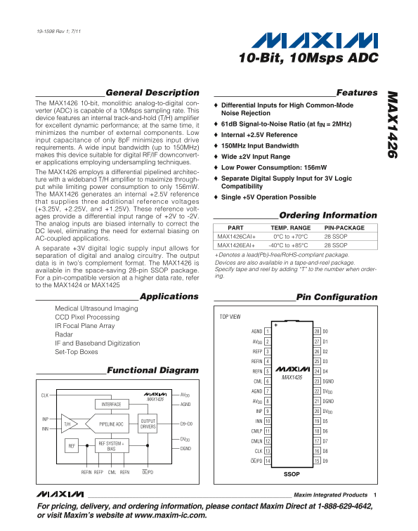
Page 1 Text Content
19-1598 Rev 1; 7/11
10-Bit, 10Msps ADC
General Description Features
The MAX1426 10-bit, monolithic analog-to-digital con-
Differential Inputs for High Common-Mode
verter (ADC) is capable of a 10Msps sampling rate. This
Noise Rejection
device features an internal track-and-hold (T/H) amplifier
for excellent dynamic performance; at the same time, it 61d B Signal-to-Noise Ratio (at f IN = 2MHz)
minimizes the number of external components. Low
Internal +2.5V Reference
input capacitance of only 8p F minimizes input drive
150MHz Input Bandwidth
requirements. A wide input bandwidth (up to 150MHz) makes this device suitable for digital RF/IF downconvert-
Wide ±2V Input Range
er applications employing undersampling techniques.
Low Power Consumption: 156m W
The MAX1426 employs a differential pipelined architec-
ture with a wideband T/H amplifier to maximize through- Separate Digital Supply Input for 3V Logic put while limiting power consumption to only 156m W. Compatibility
The MAX1426 generates an internal +2.5V reference
Single +5V Operation Possible
that supplies three additional reference voltages (+3.25V, +2.25V, and +1.25V). These reference volt-
ages provide a differential input range of +2V to -2V. Ordering Information
The analog inputs are biased internally to correct the
PART TEMP. RANGE PIN-PACKAGE
DC level, eliminating the need for external biasing on
MAX1426CAI+ 0°C to +70°C 28 SSOP
AC-coupled applications.
MAX1426EAI+ -40°C to +85°C 28 SSOP
A separate +3V digital logic supply input allows for
separation of digital and analog circuitry. The output +Denotes a lead(Pb)-free/Ro HS-compliant package. data is in two’s complement format. The MAX1426 is Devices are also available in a tape-and-reel package. available in the space-saving 28-pin SSOP package. Specify tape and reel by adding “T” to the number when order- ing.
For a pin-compatible version at a higher data rate, refer to the MAX1424 or MAX1425
Applications Pin Configuration
Medical Ultrasound Imaging
CCD Pixel Processing TOP VIEW
IR Focal Plane Array
AGND D0
Radar
AVDD D1
IF and Baseband Digitization
Set-Top Boxes REFP D2 REFIN D3 Functional Diagram REFN D4
MAX1426
CML DGND
AGND DVDD
CLK AVDD
MAX1426
AVDD DGND
INTERFACE AGND
INP DVDD
OUTPUT INN D5
T/H PIPELINE ADC D9–D0
DRIVERS
CMLP D6
CMLN D7
REF SYSTEM +
BIAS DGND
CLK D8
OE/PD D9
REFIN REFP CML REFN OE/PD
Maxim Integrated Products
For pricing, delivery, and ordering information, please contact Maxim Direct at 1-888-629-4642, or visit Maxim’s website at www.maxim-ic.com.
Page Summary Contents For MAXIM MAX1426 10-Bit, 10Msps ADC Data Sheet
Manual Details
| Brand | ADC |
|---|---|
| Pages | 16 |
| File Size | 429.94 KB |
| Published | May 13, 2026 |
Enter the captcha to get the download link:

Frequently Asked Questions
What is the maximum sampling rate of the MAX1426 ADC?
The converter is capable of a 10Msps sampling rate.
How should I ensure optimal signal integrity when using this device?
You must bypass all analog voltages (AV, REFIN, REFP, etc.) to AGND and use multilayer boards with separated ground/power planes.
Does the MAX1426 allow for single voltage supply operation?
Yes, single +5V Operation is possible.
What specific temperature range does the '-40°C to +85°C' version cover?
The device part number MAX1426EAI covers the extended temperature range of -40°C to +85°C.