MAXIM MAX1421 12-Bit, 40Msps, 3.3V Low-Power ADC with Internal Reference
Summary
The MAX1421 is a high-precision, low-power 3.3V Analog-to-Digital Converter (ADC), featuring a fully-differential input and internal precision bandgap reference for signal conversion up to 40Msps. This technical manual provides comprehensive specifications on its architecture, including power consumption modes, electrical characteristics, and operational setup. It is designed for engineers and developers building demanding electronic systems in fields such as Medical Ultrasound Imaging, Radar digitization, data acquisition, and high-speed CCD pixel processing.
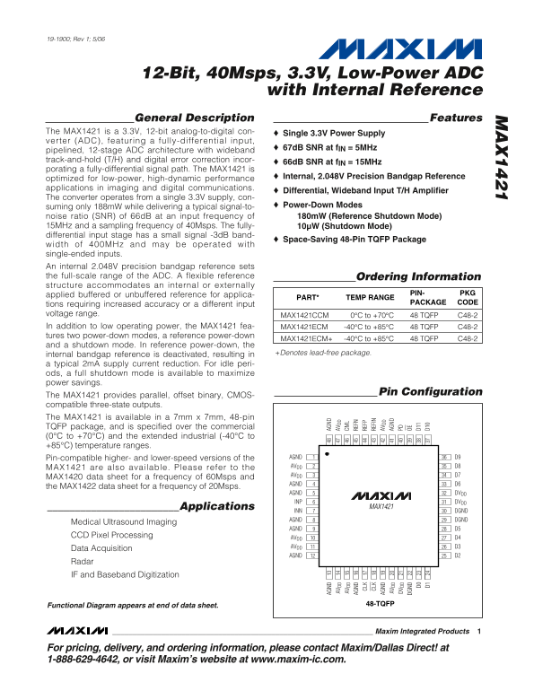
Page 1 Text Content
19-1900; Rev 1; 5/06
12-Bit, 40Msps, 3.3V, Low-Power ADC
with Internal Reference
General Description Features
The MAX1421 is a 3.3V, 12-bit analog-to-digital con- Single 3.3V Power Supply verter (ADC), featuring a fully-differential input,
67d B SNR at f IN = 5MHz
pipelined, 12-stage ADC architecture with wideband track-and-hold (T/H) and digital error correction incor-
66d B SNR at f IN = 15MHz
porating a fully-differential signal path. The MAX1421 is
Internal, 2.048V Precision Bandgap Reference
optimized for low-power, high-dynamic performance applications in imaging and digital communications.
Differential, Wideband Input T/H Amplifier
The converter operates from a single 3.3V supply, con-
suming only 188m W while delivering a typical signal-to- Power-Down Modes
noise ratio (SNR) of 66d B at an input frequency of 180m W (Reference Shutdown Mode) 15MHz and a sampling frequency of 40Msps. The fully- 10µW (Shutdown Mode) differential input stage has a small signal -3d B band-
Space-Saving 48-Pin TQFP Package
width of 400MHz and may be operated with single-ended inputs. An internal 2.048V precision bandgap reference sets the full-scale range of the ADC. A flexible reference Ordering Information structure accommodates an internal or externally
applied buffered or unbuffered reference for applica- PIN- PKG
PART* TEMP RANGE
PACKAGE CODE
tions requiring increased accuracy or a different input voltage range. M AX1421CCM 0°C to +70°C 48 TQFP C48-2 In addition to low operating power, the MAX1421 fea- M AX1421ECM -40°C to +85°C 48 TQFP C48-2
AG ND AG ND
tures two power-down modes, a reference power-down
AV DD AV DD M AX1421ECM+ -40°C to +85°C 48 TQFP C48-2
and a shutdown mode. In reference power-down, the AV CM
internal bandgap reference is deactivated, resulting in +Denotes lead-free package. AG ND RE FN
a typical 2m A supply current reduction. For idle peri- CL RE FP
ods, a full shutdown mode is available to maximize CL RE FI power savings. AG ND AV DD AV DD AG ND Pin Configuration
The MAX1421 provides parallel, offset binary, CMOS-
DV DD PD
compatible three-state outputs.
DG ND OE
The MAX1421 is available in a 7mm x 7mm, 48-pin D0 D1 TQFP package, and is specified over the commercial D1 D1 (0°C to +70°C) and the extended industrial (-40°C to +85°C) temperature ranges.
Pin-compatible higher- and lower-speed versions of the AGND D9 AVDD D8
MAX1421 are also available. Please refer to the
AVDD D7
MAX1420 data sheet for a frequency of 60Msps and
AGND D6
the MAX1422 data sheet for a frequency of 20Msps.
AGND DVDD
INP DVDD
________________________Applications MAX1421
INN DGND AGND DGND
Medical Ultrasound Imaging
AGND D5
CCD Pixel Processing
AVDD D4 AVDD D3
Data Acquisition
AGND D2
Radar IF and Baseband Digitization
Functional Diagram appears at end of data sheet. 48-TQFP
Maxim Integrated Products
For pricing, delivery, and ordering information, please contact Maxim/Dallas Direct! at 1-888-629-4642, or visit Maxim’s website at www.maxim-ic.com.
Page Summary Contents For MAXIM MAX1421 12-Bit, 40Msps, 3.3V Low-Power ADC with Internal Reference
Manual Details
| Brand | ADC |
|---|---|
| Pages | 17 |
| File Size | 572.51 KB |
| Published | May 13, 2026 |
Enter the captcha to get the download link:

Frequently Asked Questions
What is the operating frequency of the MAX1421 ADC?
The device operates up to 40 Msps.
How can I reduce the overall power consumption?
For maximum savings, utilize the full shutdown mode; otherwise, the reference power-down mode deactivates the internal bandgap reference.
What physical constraints apply regarding temperature operation?
The device is available in a commercial grade (0°C to +70°C) and an extended industrial range (-40°C to +85°C).
What voltage requirements does the ADC need for power?
The converter operates using a single 3.3V power supply.