MAXIM MAX1420 12-Bit, 60Msps, 3.3V, Low-Power ADC with Internal Reference User Manual Data Sheet
Summary
Engineered for critical digital signal processing tasks, this high-performance 12-bit Analog-to-Digital Converter (ADC) provides accurate data acquisition in challenging environments. Featuring a fully-differential input and ultra-low power operation across multiple shutdown modes, it is ideal for RF components requiring high dynamic range. The manual details technical specifications for specialized applications, including medical ultrasound, radar, imaging, and professional digital communications systems, making it essential for advanced electronics engineers.
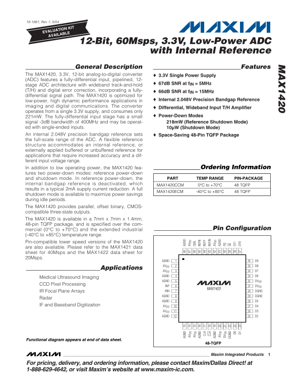
Page 1 Text Content
19-1981; Rev 1; 5/04
EVALUATION KIT AVAILABLE
12-Bit, 60Msps, 3.3V, Low-Power ADC
with Internal Reference
General Description Features
The MAX1420, 3.3V, 12-bit analog-to-digital converter 3.3V Single Power Supply (ADC) features a fully-differential input, pipelined, 12-
67d B SNR at f IN = 5MHz
stage ADC architecture with wideband track-and-hold (T/H) and digital error correction, incorporating a fully-
66d B SNR at f IN = 15MHz
differential signal path. The MAX1420 is optimized for
Internal 2.048V Precision Bandgap Reference
low-power, high dynamic performance applications in imaging and digital communications. The converter
Differential, Wideband Input T/H Amplifier
operates from a single 3.3V supply, and consumes only
221m W. The fully-differential input stage has a small Power-Down Modes
signal -3d B bandwidth of 400MHz and may be operat- 218m W (Reference Shutdown Mode) ed with single-ended inputs. 10µW (Shutdown Mode) An internal 2.048V precision bandgap reference sets Space-Saving 48-Pin TQFP Package the full-scale range of the ADC. A flexible reference structure accommodates an internal reference, or externally applied buffered or unbuffered reference for applications that require increased accuracy and a dif- ferent input voltage range.
In addition to low operating power, the MAX1420 fea- Ordering Information
tures two power-down modes: reference power-down
and shutdown mode. In reference power-down, the PART TEMP RANGE PIN-PACKAGE
internal bandgap reference is deactivated, which AG ND AG ND
MAX1420CCM 0°C to +70°C 48 TQFP results in a typical 2m A supply current reduction. A full AV DD AV DD MAX1420ECM -40°C to +85°C 48 TQFP
shutdown mode is available to maximize power savings AV DD CM during idle periods. AG ND RE FN CL RE FP
The MAX1420 provides parallel, offset binary, CMOS-
CL RE FI
compatible three-state outputs.
AG ND AV DD
The MAX1420 is available in a 7mm x 7mm x 1.4mm, AV DD AG ND
48-pin TQFP package, and is specified over the com- DV DD PD
mercial (0°C to +70°C) and the extended industrial DG ND OE Pin Configuration
(-40°C to +85°C) temperature range. D0 D1 D1 D1
Pin-compatible lower speed versions of the MAX1420 are also available. Please refer to the MAX1421 data sheet for 40Msps and the MAX1422 data sheet for 20Msps.
AGND D9 AVDD D8
________________________Applications
AVDD D7 AGND D6
Medical Ultrasound Imaging
AGND DVDD
CCD Pixel Processing
INP DVDD
MAX1420
IR Focal Plane Arrays INN DGND AGND DGND
Radar
AGND D5
IF and Baseband Digitization AVDD D4
AVDD D3 AGND D2
Functional diagram appears at end of data sheet.
48-TQFP
Maxim Integrated Products
For pricing, delivery, and ordering information, please contact Maxim/Dallas Direct! at 1-888-629-4642, or visit Maxim’s website at www.maxim-ic.com.
Page Summary Contents For MAXIM MAX1420 12-Bit, 60Msps, 3.3V, Low-Power ADC with Internal Reference User Manual Data Sheet
Manual Details
| Brand | ADC |
|---|---|
| Pages | 17 |
| File Size | 328.02 KB |
| Published | May 13, 2026 |
Enter the captcha to get the download link:

Frequently Asked Questions
What power supply voltage does the MAX1420 operate on?
It operates from a single 3.3V power supply.
How can I conserve power when the unit is idle?
Use the full shutdown mode to maximize power savings, which draws only 10µW.
Is there an option for different operating temperatures?
Yes, it is available in CCM (0°C to +70°C) and ECM (-40°C to +85°C) versions.
What does the internal reference voltage provide?
It provides a stable 2.048V precision bandgap reference for setting the ADC's full-scale range.
Does the device have multiple output types?
The MAX1420 offers parallel, offset binary, and CMOS-compatible three-state outputs.