MAXIM MAX1190 Dual 10-Bit, 120Msps, 3.3V Low-Power ADC with Internal Reference and Parallel Outputs
Summary
This technical manual details the MAX1190, a high-performance dual 10-bit Analog-to-Digital Converter (ADC). Designed for demanding applications such as medical imaging, instrumentation, and wireless communications, it delivers exceptional dynamic performance with ultra-low power consumption while operating from a single 3.3V supply. The document provides comprehensive specifications on its advanced features, including high sampling rates (120 Msps), internal precision reference structures, and multiple low-power sleep modes for optimized efficiency in professional digital circuits.
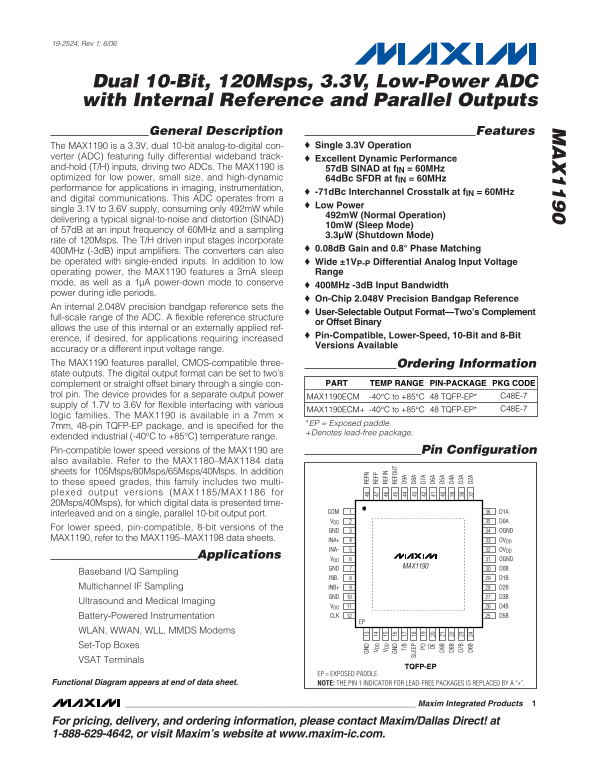
Page 1 Text Content
19-2524; Rev 1; 6/06
Dual 10-Bit, 120Msps, 3.3V, Low-Power ADC with Internal Reference and Parallel Outputs General Description Features
The MAX1190 is a 3.3V, dual 10-bit analog-to-digital con- Single 3.3V Operation
verter (ADC) featuring fully differential wideband track-
Excellent Dynamic Performance
and-hold (T/H) inputs, driving two ADCs. The MAX1190 is 57d B SINAD at f IN = 60MHz optimized for low power, small size, and high-dynamic 64d Bc SFDR at f IN = 60MHz performance for applications in imaging, instrumentation,
-71d Bc Interchannel Crosstalk at f IN = 60MHz
and digital communications. This ADC operates from a
Low Power
single 3.1V to 3.6V supply, consuming only 492m W while
492m W (Normal Operation)
delivering a typical signal-to-noise and distortion (SINAD)
10m W (Sleep Mode)
of 57d B at an input frequency of 60MHz and a sampling
3.3µW (Shutdown Mode)
rate of 120Msps. The T/H driven input stages incorporate
0.08d B Gain and 0.8° Phase Matching
400MHz (-3d B) input amplifiers. The converters can also be operated with single-ended inputs. In addition to low Wide ±1VP-P Differential Analog Input Voltage operating power, the MAX1190 features a 3m A sleep Range mode, as well as a 1µA power-down mode to conserve
400MHz -3d B Input Bandwidth
power during idle periods.
On-Chip 2.048V Precision Bandgap Reference
An internal 2.048V precision bandgap reference sets the
User-Selectable Output Format—Two’s Complement
full-scale range of the ADC. A flexible reference structure
or Offset Binary
allows the use of this internal or an externally applied ref-
Pin-Compatible, Lower-Speed, 10-Bit and 8-Bit
erence, if desired, for applications requiring increased
Versions Available
accuracy or a different input voltage range. The MAX1190 features parallel, CMOS-compatible three- Ordering Information
GN RE FN
state outputs. The digital output format can be set to two’s RE FP
complement or straight offset binary through a single con- RE FI PART TEMP RANGE PIN-PACKAGE PKG CODE
trol pin. The device provides for a separate output power GN RE FO UT C48E-7
MAX1190ECM -40°C to +85°C 48 TQFP-EP*
supply of 1.7V to 3.6V for flexible interfacing with various T/ D9
MAX1190ECM+ -40°C to +85°C 48 TQFP-EP* C48E-7
SL EE D8
logic families. The MAX1190 is available in a 7mm ✕
PD D7 *EP = Exposed paddle.
7mm, 48-pin TQFP-EP package, and is specified for the
OE D6 +Denotes lead-free package.
extended industrial (-40°C to +85°C) temperature range.
Pin-compatible lower speed versions of the MAX1190 are D8 D4 Pin Configuration
also available. Refer to the MAX1180–MAX1184 data D7 D3 sheets for 105Msps/80Msps/65Msps/40Msps. In addition D6 D2
to these speed grades, this family includes two multi- plexed output versions (MAX1185/MAX1186 for 20Msps/40Msps), for which digital data is presented time-
COM D1A
interleaved and on a single, parallel 10-bit output port.
VDD D0A
For lower speed, pin-compatible, 8-bit versions of the
GND OGND
MAX1190, refer to the MAX1195–MAX1198 data sheets. INA+ OVDD
INA- OVDD
Applications
VDD OGND
MAX1190
GND D0B
Baseband I/Q Sampling
INB- D1B
Multichannel IF Sampling INB+ D2B
GND D3B
Ultrasound and Medical Imaging
VDD D4B Battery-Powered Instrumentation CLK D5B
WLAN, WWAN, WLL, MMDS Modems Set-Top Boxes VSAT Terminals
TQFP-EP
EP = EXPOSED PADDLE.
Functional Diagram appears at end of data sheet. NOTE: THE PIN 1 INDICATOR FOR LEAD-FREE PACKAGES IS REPLACED BY A “+”.
Maxim Integrated Products
For pricing, delivery, and ordering information, please contact Maxim/Dallas Direct! at 1-888-629-4642, or visit Maxim’s website at www.maxim-ic.com.
Page Summary Contents For MAXIM MAX1190 Dual 10-Bit, 120Msps, 3.3V Low-Power ADC with Internal Reference and Parallel Outputs
Manual Details
| Brand | Dual |
|---|---|
| Pages | 22 |
| File Size | 421.67 KB |
| Published | May 30, 2026 |
Enter the captcha to get the download link:

Frequently Asked Questions
What voltage is required for the MAX1190 to operate?
The ADC operates from a single 3.1V to 3.6V supply.
How does the device manage power when idle?
It offers three modes: Sleep Mode (3mA), Low Power Range mode, and Shutdown Mode (1µA).
Does the MAX1190 support multiple input types?
Yes, it supports fully differential wideband track-and-hold inputs or single-ended inputs.
What internal reference voltage is provided?
It includes an on-chip 2.048V precision bandgap reference.