MAXIM MAX1185 Dual 10-Bit, 20Msps, 3V, Low-Power ADC with Internal Reference and Multiplexed Parallel Outputs
Summary
The MAX1185 is a high-performance, low-power dual 10-bit Analog-to-Digital Converter (ADC) operating at 20Msps. Engineered for demanding applications, it offers excellent dynamic performance and features single 3V operation with an internal reference. This guide provides comprehensive technical specifications, detailing operational modes, signal input/output configurations, absolute maximum ratings, and pin assignments. It is the perfect solution for engineers in fields such as medical imaging, video processing, instrumentation, and complex digital communication systems needing reliable, energy-efficient data conversion.
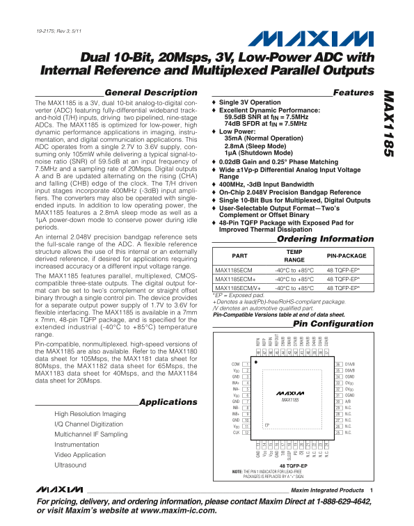
Page 1 Text Content
19-2175; Rev 3; 5/11
Dual 10-Bit, 20Msps, 3V, Low-Power ADC with Internal Reference and Multiplexed Parallel Outputs General Description Features
The MAX1185 is a 3V, dual 10-bit analog-to-digital con- Single 3V Operation verter (ADC) featuring fully-differential wideband track- Excellent Dynamic Performance:
and-hold (T/H) inputs, driving two pipelined, nine-stage 59.5d B SNR at f IN = 7.5MHz
ADCs. The MAX1185 is optimized for low-power, high 74d B SFDR at f IN = 7.5MHz dynamic performance applications in imaging, instru- Low Power: mentation, and digital communication applications. This 35m A (Normal Operation) ADC operates from a single 2.7V to 3.6V supply, con- 2.8m A (Sleep Mode) suming only 105m W while delivering a typical signal-to- 1µA (Shutdown Mode)
noise ratio (SNR) of 59.5d B at an input frequency of 0.02d B Gain and 0.25° Phase Matching 7.5MHz and a sampling rate of 20Msps. Digital outputs Wide ±1Vp-p Differential Analog Input Voltage A and B are updated alternating on the rising (CHA) Range and falling (CHB) edge of the clock. The T/H driven 400MHz, -3d B Input Bandwidth input stages incorporate 400MHz (-3d B) input ampli-
On-Chip 2.048V Precision Bandgap Reference
fiers. The converters may also be operated with single-
Single 10-Bit Bus for Multiplexed, Digital Outputs
ended inputs. In addition to low operating power, the
User-Selectable Output Format—Two’s
MAX1185 features a 2.8m A sleep mode as well as a
Complement or Offset Binary
1µA power-down mode to conserve power during idle
48-Pin TQFP Package with Exposed Pad for
periods.
Improved Thermal Dissipation
An internal 2.048V precision bandgap reference sets
Ordering Information
the full-scale range of the ADC. A flexible reference structure allows the use of this internal or an externally TEMP
PART PIN-PACKAGE
GN RE FN
derived reference, if desired for applications requiring RANGE
RE FP
increased accuracy or a different input voltage range.
RE FI MAX1185ECM -40°C to +85°C 48 TQFP-EP*
The MAX1185 features parallel, multiplexed, CMOS- GN RE FO UT
MAX1185ECM+ -40°C to +85°C 48 TQFP-EP*
compatible three-state outputs. The digital output for- T/ D9 A/
SL EE D8 A/ MAX1185ECM/V+ -40°C to +85°C 48 TQFP-EP*
mat can be set to two’s complement or straight offset
PD D7 A/ *EP = Exposed pad.
binary through a single control pin. The device provides
OE D6 A/ +Denotes a lead(Pb)-free/Ro HS-compliant package.
for a separate output power supply of 1.7V to 3.6V for
N. C. D5 A/ /V denotes an automotive qualified part.
flexible interfacing. The MAX1185 is available in a 7mm N. C. D4 A/
Pin-Compatible Versions table at end of data sheet.
x 7mm, 48-pin TQFP package, and is specified for the N. C. D3 A/
D2 A/ Pin Configuration
extended industrial (-40°C to +85°C) temperature N. C.
range. Pin-compatible, nonmultiplexed. high-speed versions of the MAX1185 are also available. Refer to the MAX1180 data sheet for 105Msps, the MAX1181 data sheet for
COM D1A/B
80Msps, the MAX1182 data sheet for 65Msps, the
VDD D0A/B
MAX1183 data sheet for 40Msps, and the MAX1184
GND OGND
data sheet for 20Msps.
INA+ OVDD INA- OVDD VDD OGND
GND MAX1185 A/B
Applications
INB- N.C. High Resolution Imaging INB+ N.C. GND N.C.
I/Q Channel Digitization EP
VDD N.C. CLK N.C.
Multichannel IF Sampling Instrumentation Video Application Ultrasound 48 TQFP-EP
NOTE: THE PIN 1 INDICATOR FOR LEAD-FREE PACKAGES IS REPLACED BY A "+" SIGN.
Maxim Integrated Products
For pricing, delivery, and ordering information, please contact Maxim Direct at 1-888-629-4642, or visit Maxim’s website at www.maxim-ic.com.
Page Summary Contents For MAXIM MAX1185 Dual 10-Bit, 20Msps, 3V, Low-Power ADC with Internal Reference and Multiplexed Parallel Outputs
Manual Details
| Brand | Dual |
|---|---|
| Pages | 21 |
| File Size | 353.49 KB |
| Published | May 20, 2026 |
Enter the captcha to get the download link:

Frequently Asked Questions
What are the typical power consumption ratings for the MAX1185?
It operates at 35mA in Normal Operation, consumes only 2.8mA in Sleep Mode, and just 1µA in Shutdown Mode.
Does this ADC maintain accuracy across various temperatures?
The device is rated for an operating temperature range of -40°C to +85°C.
What high-level performance metrics does the MAX1185 deliver?
It offers up to 59.5dB SNR at 7.5MHz and a sampling rate of 20Msps, with a 400MHz bandwidth.
How can the user customize the input voltage range?
The ADC supports using an internal precision bandgap reference or incorporating an external reference for increased accuracy.