# A B C D E F G H I J K L M N O P Q R S T U V W X Y Z

MAXIM MAX1449 10-Bit, 105Msps, Single 3.3V, Low-Power ADC with Internal Reference

Summary

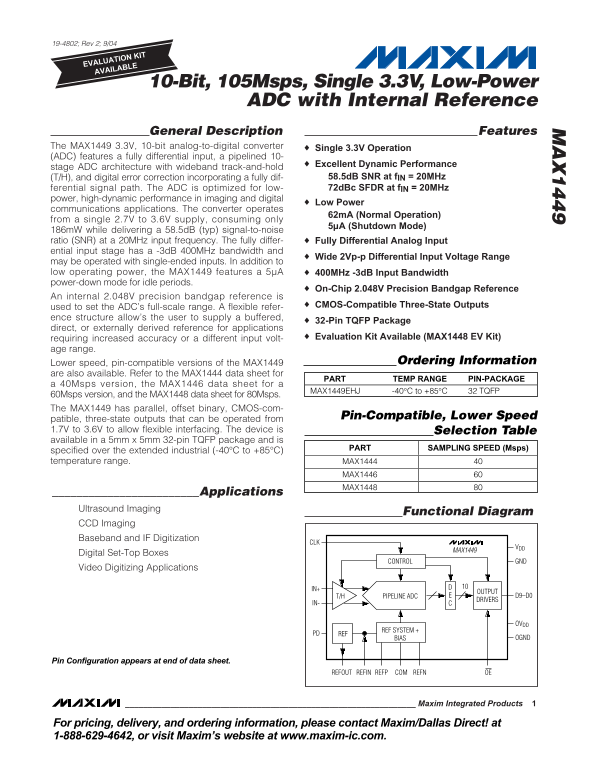
A high-speed, low-power Analog-to-Digital Converter (ADC) designed for demanding signal digitization applications. This component features 10-bit resolution at 105 Msps, making it ideal for reliable operation in imaging systems, set-top boxes, and complex digital communications. The accompanying manual provides detailed electrical specifications, operational guidelines, and integration details, serving professional engineers responsible for developing advanced test equipment or critical signal processing devices across various industrial sectors.
📄 Preview PAGE OF 21

Page 1 Text Content

19-4802; Rev 2; 9/04

EVALUATION KIT AVAILABLE

10-Bit, 105Msps, Single 3.3V, Low-Power

ADC with Internal Reference

General Description Features

The MAX1449 3.3V, 10-bit analog-to-digital converter Single 3.3V Operation (ADC) features a fully differential input, a pipelined 10-

Excellent Dynamic Performance

stage ADC architecture with wideband track-and-hold

(T/H), and digital error correction incorporating a fully dif- 58.5d B SNR at f IN = 20MHz ferential signal path. The ADC is optimized for low- 72d Bc SFDR at f IN = 20MHz

power, high-dynamic performance in imaging and digital

Low Power

communications applications. The converter operates

62m A (Normal Operation)

from a single 2.7V to 3.6V supply, consuming only

5µA (Shutdown Mode)

186m W while delivering a 58.5d B (typ) signal-to-noise ratio (SNR) at a 20MHz input frequency. The fully differ- Fully Differential Analog Input ential input stage has a -3d B 400MHz bandwidth and

Wide 2Vp-p Differential Input Voltage Range

may be operated with single-ended inputs. In addition to low operating power, the MAX1449 features a 5µA 400MHz -3d B Input Bandwidth power-down mode for idle periods.

On-Chip 2.048V Precision Bandgap Reference

An internal 2.048V precision bandgap reference is

used to set the ADC’s full-scale range. A flexible refer- CMOS-Compatible Three-State Outputs

ence structure allow’s the user to supply a buffered,

32-Pin TQFP Package

direct, or externally derived reference for applications

requiring increased accuracy or a different input volt- Evaluation Kit Available (MAX1448 EV Kit)

age range.

Lower speed, pin-compatible versions of the MAX1449 Ordering Information

are also available. Refer to the MAX1444 data sheet for

PART TEMP RANGE PIN-PACKAGE

a 40Msps version, the MAX1446 data sheet for a

MAX1449EHJ -40°C to +85°C 32 TQFP

60Msps version, and the MAX1448 data sheet for 80Msps. The MAX1449 has parallel, offset binary, CMOS-com-

Pin-Compatible, Lower Speed

patible, three-state outputs that can be operated from 1.7V to 3.6V to allow flexible interfacing. The device is Selection Table available in a 5mm x 5mm 32-pin TQFP package and is

PART SAMPLING SPEED (Msps)

specified over the extended industrial (-40°C to +85°C) temperature range. MAX1444

MAX1446 MAX1448

________________________Applications Ultrasound Imaging

Functional Diagram

CCD Imaging Baseband and IF Digitization

MAX1449

Digital Set-Top Boxes

CONTROL GND

Video Digitizing Applications

OUTPUT

T/H PIPELINE ADC D9–D0

DRIVERS

REF SYSTEM +

PD REF

BIAS OGND

Pin Configuration appears at end of data sheet.

REFINREFOUT REFP COM REFN OE

Maxim Integrated Products

For pricing, delivery, and ordering information, please contact Maxim/Dallas Direct! at 1-888-629-4642, or visit Maxim’s website at www.maxim-ic.com.

Page Summary Contents For MAXIM MAX1449 10-Bit, 105Msps, Single 3.3V, Low-Power ADC with Internal Reference

Page 1 19-4802; Rev 2; 9/04 EVALUATION KIT AVAILABLE 10-Bit, 105Msps, Single 3.3V, Low-Power ADC with Internal Reference General Description Features The MAX1449 3.3V, 10-bit analog-to-digital converter Sing...
Page 2 10-Bit, 105Msps, Single 3.3V, Low-Power ADC with Internal Reference ABSOLUTE MAXIMUM RATINGS VDD, OVDD to GND ...............................................-0.3V to +3.6V Continuous Power Dissipation...
Page 3 10-Bit, 105Msps, Single 3.3V, Low-Power ADC with Internal Reference ELECTRICAL CHARACTERISTICS (continued) (VDD = 3.3V, OVDD = 2V, 0.1µF and 1µF capacitors from REFP, REFN, and COM to GND, VREFIN = 2....
Page 4 10-Bit, 105Msps, Single 3.3V, Low-Power ADC with Internal Reference ELECTRICAL CHARACTERISTICS (continued) (VDD = 3.3V, OVDD = 2V, 0.1µF and 1µF capacitors from REFP, REFN, and COM to GND, VREFIN = 2....
Page 5 10-Bit, 105Msps, Single 3.3V, Low-Power ADC with Internal Reference ELECTRICAL CHARACTERISTICS (continued) (VDD = 3.3V, OVDD = 2V, 0.1µF and 1µF capacitors from REFP, REFN, and COM to GND, VREFIN = 2....
Page 6 SF DR (d Bc AM PL IT UD (d B) AM PL IT UD (d B) 10-Bit, 105Msps, Single 3.3V, Low-Power ADC with Internal Reference Typical Operating Characteristics (VDD = 3.3V, OVDD = 2.0V, internal reference, diff...
Page 7 SI NA (d B) SI NA (d B) SF DR (d Bc 10-Bit, 105Msps, Single 3.3V, Low-Power ADC with Internal Reference Typical Operating Characteristics (continued) (VDD = 3.3V, OVDD = 2.0V, internal reference, diff...
Page 8 DN (L SB DD (m A) TH (d Bc 10-Bit, 105Msps, Single 3.3V, Low-Power ADC with Internal Reference Typical Operating Characteristics (continued) (VDD = 3.3V, OVDD = 2.0V, internal reference, differential ...
Page 9 VD (m A) 10-Bit, 105Msps, Single 3.3V, Low-Power ADC with Internal Reference Typical Operating Characteristics (continued) SN R/ SI NA D, HD /S FD (d B, Bc EF OU T ( V) (VDD = 3.3V, OVDD = 2.0V, inter...
Page 10 10-Bit, 105Msps, Single 3.3V, Low-Power ADC with Internal Reference Pin Description PIN NAME FUNCTION Lower Reference. Conversion range is ±(VREFP - VREFN). Bypass to GND with a > 0.1µF capacitor. ...
Page 11 10-Bit, 105Msps, Single 3.3V, Low-Power ADC with Internal Reference Detailed Description and open simultaneously with S1, sampling the input waveform. Switches S4a and S4b are then opened The MAX1449 ...
Page 12 10-Bit, 105Msps, Single 3.3V, Low-Power ADC with Internal Reference The MAX1449 provides three modes of reference oper- Clock jitter is especially critical for undersampling ation: applications. The c...
Page 13 10-Bit, 105Msps, Single 3.3V, Low-Power SN (d B) SF DR (d Bc ADC with Internal Reference -50 f IN = 25.123MHz AT -0.5d B FS f IN = 25.123MHz AT -0.5d B FS -55 CLOCK DUTY CYCLE (%) CLOCK DUTY CYCLE (%)...
Page 14 10-Bit, 105Msps, Single 3.3V, Low-Power ADC with Internal Reference System Timing Requirements Using Transformer Coupling Figure 6 depicts the relationship between the clock An RF transformer (Figure ...
Page 15 10-Bit, 105Msps, Single 3.3V, Low-Power ADC with Internal Reference 5V LOWPASS FILTER MAX4108 300Ω 0.1µF RISO MAX1449 INPUT LOWPASS FILTER MAX4108 MAX4108 Figure 7. Typical Application Circuit Using t...
Page 16 10-Bit, 105Msps, Single 3.3V, Low-Power ADC with Internal Reference REFOUT29N.C. REFIN31 REFP32 MAX1449 N = 1 REFN1 MAX6062 1µF MAX4250 COM2 10Hz LOWPASS FILTER 10Hz LOWPASS FILTER REFOUT29N.C. REFIN3...
Page 17 10-Bit, 105Msps, Single 3.3V, Low-Power ADC with Internal Reference REFOUT29N.C. REFIN31 REFP32 MAX1449 2.0V AT 8m A N = 1 MAX6066 47Ω REFN1 1/4 MAX4252 3.3V 1.5V AT 0m A 1/4 MAX4252 MAX4254 POWER-SUP...
Page 18 10-Bit, 105Msps, Single 3.3V, Low-Power ADC with Internal Reference Grounding, Bypassing, Dynamic Parameter Definitions and Board Layout Aperture Jitter Figure 12 depicts the aperture jitter (t AJ), w...
Page 19 10-Bit, 105Msps, Single 3.3V, Low-Power ADC with Internal Reference Pin Configuration TOP VIEW ANALOG INPUT t AD 1REFN D4 COM OGND SAMPLED DATA (T/H) VDD T.P. GND OVDD MAX1449 TRACK HOLD TRACK GND D5 ...
Page 20 10-Bit, 105Msps, Single 3.3V, Low-Power ADC with Internal Reference Package Information (The package drawing(s) in this data sheet may not reflect the most current specifications. For the latest packa...
Page 21 10-Bit, 105Msps, Single 3.3V, Low-Power ADC with Internal Reference Package Information (continued) (The package drawing(s) in this data sheet may not reflect the most current specifications. For the ...

Manual Details

Brand ADC
Pages 21
File Size 358.28 KB
Published May 13, 2026
165 views

Enter the captcha to get the download link:

captcha

Frequently Asked Questions

What is the ADC's power consumption in normal and shutdown modes?

In normal operation, it consumes 62mA; however, in shutdown mode, it only uses 5µA.

Are there lower speed, pin-compatible versions of this MAX1449?

Yes, models such as the MAX1444 (40Msps), MAX1446 (60Msps), and MAX1448 (80Msps) are available.

How can I set or modify the ADC's full-scale range for my application?

The device uses an internal 2.048V reference, but users can supply a buffered, direct, or externally derived reference.

What is the bandwidth and general voltage range of the differential analog input?

The fully differential input stage has a -3dB 400MHz bandwidth and supports a wide 2Vp-p differential input voltage range.