MAXIM MAX19516 Dual-Channel, 10-Bit, 100Msps ADC Data Sheet
Summary
This high-performance MAX19516 is a dual-channel, 10-bit Analog-to-Digital Converter capable of up to 100Msps sampling rate while maintaining very low power consumption. Designed for precision data acquisition, it features an extremely wide input common-mode voltage range and high dynamic performance, making it ideal for IF and baseband communications, medical imaging, and portable instrumentation. The technical manual provides comprehensive specifications, pin configurations, and operational details required to integrate this advanced ADC into sophisticated low-power systems.
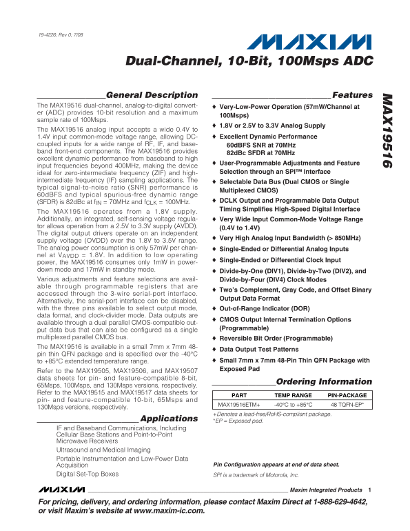
Page 1 Text Content
19-4226; Rev 0; 7/08
Dual-Channel, 10-Bit, 100Msps ADC
General Description Features
The MAX19516 dual-channel, analog-to-digital convert- Very-Low-Power Operation (57m W/Channel at er (ADC) provides 10-bit resolution and a maximum
100Msps)
sample rate of 100Msps.
1.8V or 2.5V to 3.3V Analog Supply
The MAX19516 analog input accepts a wide 0.4V to
1.4V input common-mode voltage range, allowing DC- Excellent Dynamic Performance
coupled inputs for a wide range of RF, IF, and base- 60d BFS SNR at 70MHz band front-end components. The MAX19516 provides
82d Bc SFDR at 70MHz
excellent dynamic performance from baseband to high
User-Programmable Adjustments and Feature
input frequencies beyond 400MHz, making the device
ideal for zero-intermediate frequency (ZIF) and high- Selection through an SPI™ Interface
intermediate frequency (IF) sampling applications. The
Selectable Data Bus (Dual CMOS or Single
typical signal-to-noise ratio (SNR) performance is
Multiplexed CMOS)
60d BFS and typical spurious-free dynamic range
(SFDR) is 82d Bc at f IN = 70MHz and f CLK = 100MHz. DCLK Output and Programmable Data Output Timing Simplifies High-Speed Digital Interface
The MAX19516 operates from a 1.8V supply. Additionally, an integrated, self-sensing voltage regula- Very Wide Input Common-Mode Voltage Range tor allows operation from a 2.5V to 3.3V supply (AVDD).
(0.4V to 1.4V)
The digital output drivers operate on an independent
Very High Analog Input Bandwidth (> 850MHz)
supply voltage (OVDD) over the 1.8V to 3.5V range. The analog power consumption is only 57m W per chan- Single-Ended or Differential Analog Inputs nel at VAVDD = 1.8V. In addition to low operating
Single-Ended or Differential Clock Input
power, the MAX19516 consumes only 1m W in power- down mode and 17m W in standby mode.
Divide-by-One (DIV1), Divide-by-Two (DIV2), and
Various adjustments and feature selections are avail- Divide-by-Four (DIV4) Clock Modes able through programmable registers that are
Two’s Complement, Gray Code, and Offset Binary
accessed through the 3-wire serial-port interface.
Output Data Format
Alternatively, the serial-port interface can be disabled, with the three pins available to select output mode, Out-of-Range Indicator (DOR) data format, and clock-divider mode. Data outputs are
CMOS Output Internal Termination Options
available through a dual parallel CMOS-compatible out-
(Programmable)
put data bus that can also be configured as a single multiplexed parallel CMOS bus. Reversible Bit Order (Programmable) The MAX19516 is available in a small 7mm x 7mm 48-
Data Output Test Patterns
pin thin QFN package and is specified over the -40°C
to +85°C extended temperature range. Small 7mm x 7mm 48-Pin Thin QFN Package with Exposed Pad
Refer to the MAX19505, MAX19506, and MAX19507 data sheets for pin- and feature-compatible 8-bit,
Ordering Information
65Msps, 100Msps, and 130Msps versions, respectively. Refer to the MAX19515 and MAX19517 data sheets for
PART TEMP RANGE PIN-PACKAGE
pin- and feature-compatible 10-bit, 65Msps and
MAX19516ETM+ -40°C to +85°C 48 TQFN-EP*
130Msps versions, respectively.
+Denotes a lead-free/Ro HS-compliant package.
Applications
*EP = Exposed pad.
IF and Baseband Communications, Including Cellular Base Stations and Point-to-Point Microwave Receivers Ultrasound and Medical Imaging Portable Instrumentation and Low-Power Data
Acquisition Pin Configuration appears at end of data sheet.
Digital Set-Top Boxes SPI is a trademark of Motorola, Inc.
Maxim Integrated Products
For pricing, delivery, and ordering information, please contact Maxim Direct at 1-888-629-4642, or visit Maxim’s website at www.maxim-ic.com.
Page Summary Contents For MAXIM MAX19516 Dual-Channel, 10-Bit, 100Msps ADC Data Sheet
Manual Details
| Brand | Dual |
|---|---|
| Pages | 34 |
| File Size | 398.49 KB |
| Published | May 30, 2026 |
Enter the captcha to get the download link:

Frequently Asked Questions
What voltage range can the MAX19516 use for its analog supply (AVDD)?
The analog input accepts a wide range from 0.4V to 1.4V, operating with VDD between 1.8V or 2.5V and 3.3V.
How can the device's output data format be customized?
The serial-port interface allows selection of multiple output modes, including CMOS Output, DOR data format, and clock-divider mode.
What is the maximum sampling rate and resolution advertised for this ADC?
It provides 10-bit resolution with a maximum sample rate of 100 Msps.
Is the device suitable for high-speed signal processing due to its bandwidth?
Yes, it features a very high analog input bandwidth, exceeding 850MHz.