# A B C D E F G H I J K L M N O P Q R S T U V W X Y Z

MAXIM MAX1191 Ultra-Low-Power, 7.5Msps, Dual 8-Bit ADC User Manual Data Sheet

Summary

This comprehensive technical guide details the MAX1191, an ultra-low-power dual 8-bit Analog-to-Digital Converter (ADC). The device is engineered for demanding applications requiring high precision and minimal power consumption, such as medical instrumentation, battery-powered portable devices, and advanced imaging. This documentation covers detailed electrical specifications, pin configurations, operating modes (including internal/external reference options), absolute maximum ratings, and best practices for integrating this efficient 7.5 Msps ADC into professional electronic designs.
📄 Preview PAGE OF 27

Page 1 Text Content

19-2836; Rev 1; 9/03

Ultra-Low-Power, 7.5Msps, Dual 8-Bit ADC General Description Features

The MAX1191 is an ultra-low-power, dual, 8-bit, Ultra-Low Power 7.5Msps analog-to-digital converter (ADC). The device

12m W (Normal Operation: 7.5Msps)

features two fully differential wideband track-and-hold

0.3µW (Shutdown Mode)

(T/H) inputs. These inputs have a 440MHz bandwidth

Excellent Dynamic Performance

and accept fully differential or single-ended signals.

The MAX1191 delivers a typical signal-to-noise and dis- 48.7d B SNR at f IN = 1.875MHz

tortion (SINAD) of 48.6d B at an input frequency of 69d Bc SFDR at f IN = 1.875MHz 1.875MHz and a sampling rate of 7.5Msps while con-

2.7V to 3.6V Single Analog Supply

suming only 12m W. This ADC operates from a 2.7V to

1.8V to 3.6V TTL/CMOS-Compatible Digital

3.6V analog power supply. A separate 1.8V to 3.6V

supply powers the digital output driver. In addition to Outputs

ultra-low operating power, the MAX1191 features three Fully Differential or Single-Ended Analog Inputs power-down modes to conserve power during idle peri-

Internal/External Reference Option

ods. Excellent dynamic performance, ultra-low power, and small size make the MAX1191 ideal for applica- Multiplexed CMOS-Compatible Tri-State Outputs tions in imaging, instrumentation, and digital communi-

28-Pin Thin QFN Package

cations.

Evaluation Kit Available (Order MAX1193EVKIT)

An internal 1.024V precision bandgap reference sets the full-scale range of the ADC to ±0.512V. A flexible

Ordering Information

reference structure allows the MAX1191 to use its inter- nal reference or accept an externally applied reference

PART TEMP RANGE PIN-PACKAGE

for applications requiring increased accuracy.

28 Thin QFN-EP*

The MAX1191 features parallel, multiplexed, CMOS- MAX1191ETI-T -40°C to +85°C

RE FP (5mm x 5mm)

compatible tri-state outputs. The digital output format is

offset binary. A separate digital power input accepts a RE FN *EP = Exposed paddle.

voltage from 1.8V to 3.6V for flexible interfacing to dif-

OG NDGN CO

ferent logic levels. The MAX1191 is available in a 5mm 5mm, 28-pin thin QFN package, and is specified for

OV DD RE FI

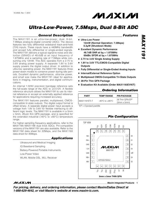
the extended industrial (-40°C to +85°C) temperature Pin Configuration

range. PD

For higher sampling frequency applications, refer to the TOP VIEW

D6D7 PD

MAX1195–MAX1198 dual 8-bit ADCs. Pin-compatible versions of the MAX1191 are also available. Refer to the MAX1192 data sheet for 22Msps, and the MAX1193 data sheet for 45Msps.

INA- D0

Applications

INA+ D1

Ultrasound and Medical Imaging

GND D2

IQ Baseband Sampling

CLK D3

Battery-Powered Portable Instruments MAX1191

GND A/B

Low-Power Video

WLAN, Mobile DSL, WLL Receiver INB+ D4

EXPOSED PADDLE

INB- D5

5mm x 5mm THIN QFN

Maxim Integrated Products

For pricing, delivery, and ordering information, please contact Maxim/Dallas Direct! at 1-888-629-4642, or visit Maxim’s website at www.maxim-ic.com.

Page Summary Contents For MAXIM MAX1191 Ultra-Low-Power, 7.5Msps, Dual 8-Bit ADC User Manual Data Sheet

Page 1 19-2836; Rev 1; 9/03 Ultra-Low-Power, 7.5Msps, Dual 8-Bit ADC General Description Features The MAX1191 is an ultra-low-power, dual, 8-bit, Ultra-Low Power 7.5Msps analog-to-digital converter (ADC). Th...
Page 2 Ultra-Low-Power, 7.5Msps, Dual 8-Bit ADC ABSOLUTE MAXIMUM RATINGS VDD, OVDD to GND ...............................................-0.3V to +3.6V Operating Temperature Range ..............................
Page 3 Ultra-Low-Power, 7.5Msps, Dual 8-Bit ADC ELECTRICAL CHARACTERISTICS (continued) (VDD = 3.0V, OVDD = 1.8V, VREFIN = VDD (internal reference), CL 10p F at digital outputs, f CLK = 7.5MHz, CREFP = CREFN ...
Page 4 Ultra-Low-Power, 7.5Msps, Dual 8-Bit ADC ELECTRICAL CHARACTERISTICS (continued) (VDD = 3.0V, OVDD = 1.8V, VREFIN = VDD (internal reference), CL 10p F at digital outputs, f CLK = 7.5MHz, CREFP = CREFN ...
Page 5 Ultra-Low-Power, 7.5Msps, Dual 8-Bit ADC ELECTRICAL CHARACTERISTICS (continued) (VDD = 3.0V, OVDD = 1.8V, VREFIN = VDD (internal reference), CL 10p F at digital outputs, f CLK = 7.5MHz, CREFP = CREFN ...
Page 6 AM PL IT UD (d B) Ultra-Low-Power, 7.5Msps, Dual 8-Bit ADC AM PL IT UD (d B) ELECTRICAL CHARACTERISTICS (continued) (VDD = 3.0V, OVDD = 1.8V, VREFIN = VDD (internal reference), CL 10p F at digital out...
Page 7 Ultra-Low-Power, 7.5Msps, Dual 8-Bit ADC AM PL IT UD (d B) AM PL IT UD (d B) Typical Operating Characteristics (continued) (VDD = 3.0V, OVDD = 1.8V, VREFIN = VDD (internal reference), CL 10p F at digi...
Page 8 TH (d B) SN (d B) Ultra-Low-Power, 7.5Msps, Dual 8-Bit ADC Typical Operating Characteristics (continued) (VDD = 3.0V, OVDD = 1.8V, VREFIN = VDD (internal reference), CL 10p F at digital outputs, diffe...
Page 9 TH (d Bc SN (d B) Ultra-Low-Power, 7.5Msps, Dual 8-Bit ADC Typical Operating Characteristics (continued) (VDD = 3.0V, OVDD = 1.8V, VREFIN = VDD (internal reference), CL 10p F at digital outputs, diffe...
Page 10 TH (d Bc SN (d B) Ultra-Low-Power, 7.5Msps, Dual 8-Bit ADC Typical Operating Characteristics (continued) (VDD = 3.0V, OVDD = 1.8V, VREFIN = VDD (internal reference), CL 10p F at digital outputs, diffe...
Page 11 TH (d Bc SN (d B) Ultra-Low-Power, 7.5Msps, Dual 8-Bit ADC Typical Operating Characteristics (continued) (VDD = 3.0V, OVDD = 1.8V, VREFIN = VDD (internal reference), CL 10p F at digital outputs, diffe...
Page 12 GA IN (d B) Ultra-Low-Power, 7.5Msps, Dual 8-Bit ADC OF FS ET RR OR S) IN (L SB Typical Operating Characteristics (continued) (VDD = 3.0V, OVDD = 1.8V, VREFIN = VDD (internal reference), CL 10p F at d...
Page 13 DI GI TA SU PP LY UR RE NT (m A) Ultra-Low-Power, 7.5Msps, Dual 8-Bit ADC Typical Operating Characteristics (continued) (VDD = 3.0V, OVDD = 1.8V, VREFIN = VDD (internal reference), CL 10p F at digital...
Page 14 Ultra-Low-Power, 7.5Msps, Dual 8-Bit ADC Pin Description (continued) PIN NAME FUNCTION PD0 Power-Down Digital Input 0. See Table 3. REFIN Reference Input. Internally pulled up to VDD. COM Common-Mode ...
Page 15 Ultra-Low-Power, 7.5Msps, Dual 8-Bit ADC INTERNAL BIAS COM INTERNAL COM BIAS HOLD HOLD INTERNAL INTERNAL COM TRACK TRACK NONOVERLAPPING CLOCK SIGNALS MAX1191 INTERNAL COM BIAS Figure 3. Internal T/H C...
Page 16 Ultra-Low-Power, 7.5Msps, Dual 8-Bit ADC Table 1. Reference Modes VREFIN REFERENCE MODE Internal reference mode. VREF is internally generated to be 0.512V. Bypass REFP, REFN, and COM >0.8 x VDD eac...
Page 17 Ultra-Low-Power, 7.5Msps, Dual 8-Bit ADC 5 CLOCK-CYCLE LATENCY (CHA), 5.5 CLOCK-CYCLE LATENCY (CHB) t CLK t CL t CH t DOB t DOA A/B CHB CHA CHB CHA CHB CHA CHB CHA CHB CHA CHB CHA CHB t DA/B OF FS ET ...
Page 18 Ultra-Low-Power, 7.5Msps, Dual 8-Bit ADC Table 2. Output Codes vs. Input Voltage DIFFERENTIAL INPUT VOLTAGE DIFFERENTIAL INPUT OFFSET BINARY OUTPUT DECIMAL CODE (IN+ - IN-) (LSB) (D7–D0) VREF 1111 111...
Page 19 Ultra-Low-Power, 7.5Msps, Dual 8-Bit ADC MAX1191 RISO 22Ω R1 INA- 600Ω CIN 5p F VCOM = 0.5V TO 1.5V VSIG = ±85m VP-P R6 R7 600Ω 600Ω COM AV = 6V/V VCOM = VDD/2 RISO 22Ω INA+ CIN 5p F OPERATIONAL AMPLI...
Page 20 Ultra-Low-Power, 7.5Msps, Dual 8-Bit ADC 25Ω REFP 1kΩ RISO T1 INA+ MAX4108 CIN N.C. COM REFN 0.1µF MINICIRCUITS TT1-6-KK81 INA- INA- MAX1191 25Ω REFP MAX1191 1kΩ RISO VIN 0.1µF T1 INB+ MAX4108 CIN REF...
Page 21 Ultra-Low-Power, 7.5Msps, Dual 8-Bit ADC VDD REFIN REFP N = 1 MAX6061 10Hz 0.33µF LOWPASS MAX1191 FILTER COM 3V GND 1.023VNOTE: ONE FRONT-END REFERENCE CIRCUIT PROVIDES ±15m A OF OUTPUT 15Ω DRIVE AND ...
Page 22 Ultra-Low-Power, 7.5Msps, Dual 8-Bit ADC MAX6066 MAX1191 1/4 47Ω REFN REFIN MAX4254 6V1µF COM 0.33µF GNDNOTE: ONE FRONT-END REFERENCE CIRCUIT SUPPORTS UP TO 160 MAX1191s. MAX4254 UNCOMMITTED 10.0kΩ VD...
Page 23 Ultra-Low-Power, 7.5Msps, Dual 8-Bit ADC MAX2451 INA+ INA- MAX1191 POST- PROCESSING INB+ INB- DOWNCONVERTER Figure 12. Typical QAM Receiver Application Typical QAM Demodulation Application ably on the...
Page 24 Ultra-Low-Power, 7.5Msps, Dual 8-Bit ADC Dynamic Parameter Definitions CLK Aperture Jitter Figure 13 depicts the aperture jitter (t AJ), which is the sample-to-sample variation in the aperture delay. ...
Page 25 Ultra-Low-Power, 7.5Msps, Dual 8-Bit ADC Total Harmonic Distortion (THD) Third-Order Intermodulation (IM3) THD is typically the ratio of the RMS sum of the first five IM3 is the power of the worst thi...
Page 26 Ultra-Low-Power, 7.5Msps, Dual 8-Bit ADC Package Information (The package drawing(s) in this data sheet may not reflect the most current specifications. For the latest package outline information go t...
Page 27 Ultra-Low-Power, 7.5Msps, Dual 8-Bit ADC Package Information (continued) (The package drawing(s) in this data sheet may not reflect the most current specifications. For the latest package outline info...