# A B C D E F G H I J K L M N O P Q R S T U V W X Y Z

MAXIM MAX19506 Dual-Channel, 8-Bit, 100Msps ADC Owner's Manual & User Guide

Summary

The MAX19506 is a powerful, dual-channel 8-bit ADC featuring excellent dynamic performance and very low power consumption. With a high sampling rate of 100 Msps, this converter provides superior digital signal acquisition capabilities for complex electrical systems. This manual serves as the comprehensive technical reference for hardware designers, detailing specifications, operating guidelines, pin definitions, and programming interfaces (SPI™). It is ideal for engineers developing sophisticated communication equipment, including cellular base stations, IF/baseband receivers, medical imaging systems, and portable instrumentation requiring wide input voltage ranges.
📄 Preview PAGE OF 35

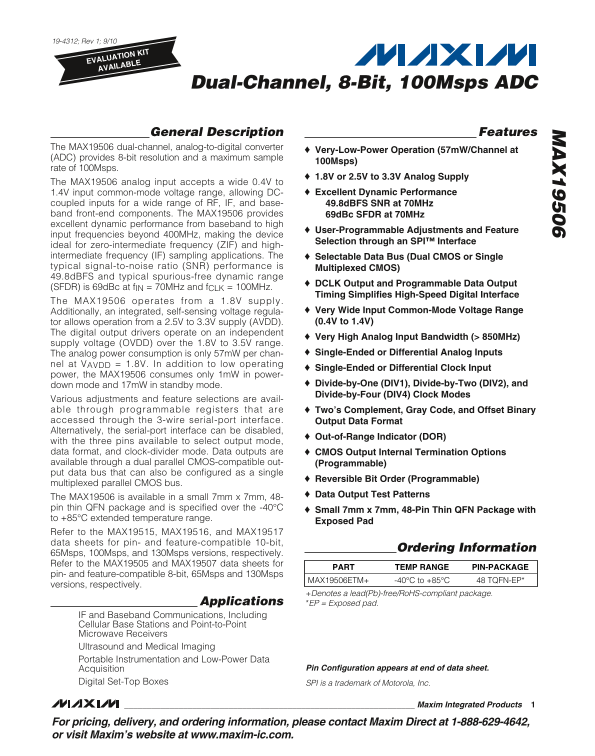
Page 1 Text Content

19-4312; Rev 1; 9/10

EVALUATION KIT AVAILABLE

Dual-Channel, 8-Bit, 100Msps ADC

General Description Features

The MAX19506 dual-channel, analog-to-digital converter

Very-Low-Power Operation (57m W/Channel at

(ADC) provides 8-bit resolution and a maximum sample

100Msps)

rate of 100Msps.

1.8V or 2.5V to 3.3V Analog Supply

The MAX19506 analog input accepts a wide 0.4V to

1.4V input common-mode voltage range, allowing DC- Excellent Dynamic Performance

coupled inputs for a wide range of RF, IF, and base- 49.8d BFS SNR at 70MHz band front-end components. The MAX19506 provides 69d Bc SFDR at 70MHz excellent dynamic performance from baseband to high

User-Programmable Adjustments and Feature

input frequencies beyond 400MHz, making the device

Selection through an SPI™ Interface

ideal for zero-intermediate frequency (ZIF) and high- intermediate frequency (IF) sampling applications. The Selectable Data Bus (Dual CMOS or Single typical signal-to-noise ratio (SNR) performance is Multiplexed CMOS) 49.8d BFS and typical spurious-free dynamic range

DCLK Output and Programmable Data Output

(SFDR) is 69d Bc at f IN = 70MHz and f CLK = 100MHz.

Timing Simplifies High-Speed Digital Interface

The MAX19506 operates from a 1.8V supply.

Additionally, an integrated, self-sensing voltage regula- Very Wide Input Common-Mode Voltage Range tor allows operation from a 2.5V to 3.3V supply (AVDD). (0.4V to 1.4V)

The digital output drivers operate on an independent

Very High Analog Input Bandwidth (> 850MHz)

supply voltage (OVDD) over the 1.8V to 3.5V range.

The analog power consumption is only 57m W per chan- Single-Ended or Differential Analog Inputs

nel at VAVDD = 1.8V. In addition to low operating

Single-Ended or Differential Clock Input

power, the MAX19506 consumes only 1m W in power-

down mode and 17m W in standby mode. Divide-by-One (DIV1), Divide-by-Two (DIV2), and Divide-by-Four (DIV4) Clock Modes

Various adjustments and feature selections are avail- able through programmable registers that are Two’s Complement, Gray Code, and Offset Binary accessed through the 3-wire serial-port interface. Output Data Format Alternatively, the serial-port interface can be disabled,

Out-of-Range Indicator (DOR)

with the three pins available to select output mode, data format, and clock-divider mode. Data outputs are CMOS Output Internal Termination Options available through a dual parallel CMOS-compatible out- (Programmable) put data bus that can also be configured as a single

Reversible Bit Order (Programmable)

multiplexed parallel CMOS bus.

Data Output Test Patterns

The MAX19506 is available in a small 7mm x 7mm, 48- pin thin QFN package and is specified over the -40°C

Small 7mm x 7mm, 48-Pin Thin QFN Package with

to +85°C extended temperature range.

Exposed Pad

Refer to the MAX19515, MAX19516, and MAX19517 data sheets for pin- and feature-compatible 10-bit,

Ordering Information

65Msps, 100Msps, and 130Msps versions, respectively. Refer to the MAX19505 and MAX19507 data sheets for

PART TEMP RANGE PIN-PACKAGE

pin- and feature-compatible 8-bit, 65Msps and 130Msps

MAX19506ETM+ -40°C to +85°C 48 TQFN-EP*

versions, respectively.

+Denotes a lead(Pb)-free/Ro HS-compliant package.

Applications *EP = Exposed pad.

IF and Baseband Communications, Including Cellular Base Stations and Point-to-Point Microwave Receivers Ultrasound and Medical Imaging Portable Instrumentation and Low-Power Data

Acquisition Pin Configuration appears at end of data sheet.

Digital Set-Top Boxes SPI is a trademark of Motorola, Inc.

Maxim Integrated Products

For pricing, delivery, and ordering information, please contact Maxim Direct at 1-888-629-4642, or visit Maxim’s website at www.maxim-ic.com.

Page Summary Contents For MAXIM MAX19506 Dual-Channel, 8-Bit, 100Msps ADC Owner's Manual & User Guide

Page 1 19-4312; Rev 1; 9/10 EVALUATION KIT AVAILABLE Dual-Channel, 8-Bit, 100Msps ADC General Description Features The MAX19506 dual-channel, analog-to-digital converter Very-Low-Power Operation (57m W/Chann...
Page 2 Dual-Channel, 8-Bit, 100Msps ADC ABSOLUTE MAXIMUM RATINGS OVDD, AVDD to GND............................................-0.3V to +3.6V 48-Pin Thin QFN, 7mm x 7mm x 0.8mm (derate 40m W/°C CMA, CMB, REFI...
Page 3 Dual-Channel, 8-Bit, 100Msps ADC ELECTRICAL CHARACTERISTICS (continued) (VAVDD = VOVDD = 1.8V, internal reference, differential clock, VCLK = 1.5VP-P, f CLK = 100MHz, AIN = -0.5d BFS, data output term...
Page 4 Dual-Channel, 8-Bit, 100Msps ADC ELECTRICAL CHARACTERISTICS (continued) (VAVDD = VOVDD = 1.8V, internal reference, differential clock, VCLK = 1.5VP-P, f CLK = 100MHz, AIN = -0.5d BFS, data output term...
Page 5 Dual-Channel, 8-Bit, 100Msps ADC ELECTRICAL CHARACTERISTICS (continued) (VAVDD = VOVDD = 1.8V, internal reference, differential clock, VCLK = 1.5VP-P, f CLK = 100MHz, AIN = -0.5d BFS, data output term...
Page 6 Dual-Channel, 8-Bit, 100Msps ADC ELECTRICAL CHARACTERISTICS (continued) (VAVDD = VOVDD = 1.8V, internal reference, differential clock, VCLK = 1.5VP-P, f CLK = 100MHz, AIN = -0.5d BFS, data output term...
Page 7 Dual-Channel, 8-Bit, 100Msps ADC ELECTRICAL CHARACTERISTICS (continued) (VAVDD = VOVDD = 1.8V, internal reference, differential clock, VCLK = 1.5VP-P, f CLK = 100MHz, AIN = -0.5d BFS, data output term...
Page 8 IN (L SB AM PL IT UD (d BF S) AM PL IT UD (d BF S) Dual-Channel, 8-Bit, 100Msps ADC Typical Operating Characteristics (VAVDD = VOVDD = 1.8V, internal reference, differential clock, VCLK = 1.5VP-P, f C...
Page 9 AN AL OG UP PL CU RR EN (m A) PE RF OR AN CE (d BF S) PE RF OR AN CE (d BF S) Dual-Channel, 8-Bit, 100Msps ADC Typical Operating Characteristics (continued) (VAVDD = VOVDD = 1.8V, internal reference, ...
Page 10 PE RF OR AN CE (d BF S) DI GI TA SU PP LY UR RE NT (m A) AN AL OG UP PL CU RR EN (m A) Dual-Channel, 8-Bit, 100Msps ADC Typical Operating Characteristics (continued) (VAVDD = VOVDD = 1.8V, internal re...
Page 11 OF FS ET RR OR (m V) Dual-Channel, 8-Bit, 100Msps ADC Typical Operating Characteristics (continued) GA IN RR OR (VAVDD = VOVDD = 1.8V, internal reference, differential clock, VCLK = 1.5VP-P, f CLK = 1...
Page 12 Dual-Channel, 8-Bit, 100Msps ADC Pin Description PIN NAME FUNCTION 1, 12, 13, 48 AVDD Analog Supply Voltage. Bypass each AVDD input pair (1, 48) and (12, 13) to GND with 0.1µF. CMA Channel A Common-Mo...
Page 13 Dual-Channel, 8-Bit, 100Msps ADC Pin Description (continued) PIN NAME FUNCTION D5A Channel A Three-State Digital Output, Bit 5 D6A Channel A Three-State Digital Output, Bit 6 D7A Channel A Three-State...
Page 14 Dual-Channel, 8-Bit, 100Msps ADC CLOCK MAX19506 INA+ DIGITAL D0A–D7A PIPELINE T/H ERROR INA- CORRECTION DORA DCLKA CMA AND OUTPUT REFERENCE INTERNAL OUTPUT DRIVERS OVDD REFIO AND BIAS REFERENCE FORMAT...
Page 15 Dual-Channel, 8-Bit, 100Msps ADC 29/32 AVDD DECODER INTERNAL GAIN—BYPASS REFIO EXTERNAL GAIN CONTROL—DRIVE REFIO 23/32 AVDD 0.1µF CS TO REFIO EXTERNAL BYPASS SCLK CONTROL SDIN LOGIC BANDGAP SCALE AND ...
Page 16 Dual-Channel, 8-Bit, 100Msps ADC SDIN R/W A6 A4A5 A2A3 A0A1 D7 D6 D4D5 D2D3 D0D1 R/W ADDRESS WRITE OR READ 0 = WRITE 1 = READ Figure 6. Serial-Interface Communication Cycle t CSH t CSS t SCLK t SDS t ...
Page 17 Dual-Channel, 8-Bit, 100Msps ADC Register address 0Ah is a special-function register. ters are reset to default values. A read operation of reg- Writing data 5Ah to register 0Ah initiates a register i...
Page 18 Dual-Channel, 8-Bit, 100Msps ADC In addition to power management, the HPS_SHDN1 The MUX_CH bit selects which bus the (A+B)/2 data is and HPS_SHDN0 activate an A+B adder mode. In this presented. mode, ...
Page 19 Dual-Channel, 8-Bit, 100Msps ADC Digital Output Power Management (02h) BIT 7 BIT 6 BIT 5 BIT 4 BIT 3 BIT 2 BIT 1 BIT 0 PD_DOUT_1 PD_DOUT_0 DIS_DOR DIS_DCLK Bit 7–4 Don’t care Bit 3, 2 PD_DOUT_1, PD_DO...
Page 20 Dual-Channel, 8-Bit, 100Msps ADC Data/DCLK Timing (03h) BIT 7 BIT 6 BIT 5 BIT 4 BIT 3 BIT 2 BIT 1 BIT 0 DA_BYPASS DLY_HALF_T DCLKTIME_2 DCLKTIME_1 DCLKTIME_0 DTIME_2 DTIME_1 DTIME_0 Bit 7 DA_BYPASS: D...
Page 21 Dual-Channel, 8-Bit, 100Msps ADC CHA Data Output Termination Control (04h) BIT 7 BIT 6 BIT 5 BIT 4 BIT 3 BIT 2 BIT 1 BIT 0 CT_DCLK_2_A CT_DCLK_1_A CT_DCLK_0_A CT_DATA_2_A CT_DATA_1_A CT_DATA_0_A Bit 7...
Page 22 Dual-Channel, 8-Bit, 100Msps ADC Clock Divide/Data Format/Test Pattern (06h) BIT 7 BIT 6 BIT 5 BIT 4 BIT 3 BIT 2 BIT 1 BIT 0 TEST_PATTERN TEST_DATA FORMAT_1 FORMAT_0 TERM_100 SYNC_MODE DIV1 DIV0 Bit 7...
Page 23 Dual-Channel, 8-Bit, 100Msps ADC Common Mode (08h) BIT 7 BIT 6 BIT 5 BIT 4 BIT 3 BIT 2 BIT 1 BIT 0 CMI_SELF_B CMI_ADJ_2_B CMI_ADJ_1_B CMI_ADJ_0_B CMI_SELF_A CMI_ADJ_2_A CMI_ADJ_1_A CMI_ADJ_0_A Bit 7 C...
Page 24 Dual-Channel, 8-Bit, 100Msps ADC 100Ω Clock Inputs TERMINATION The input clock interface provides for flexibility in the (PROGRAMMABLE) requirements of the clock driver. The MAX19506 CLK+ 2:1 MUX AVDD...
Page 25 Dual-Channel, 8-Bit, 100Msps ADC MUX OUTPUT MODE SAMPLING INSTANT SAMPLING SAMPLING SAMPLING INSTANT t AD INSTANT INSTANT SAMPLING SAMPLING INSTANT IN_ INSTANT t CLK t CH t CLSAMPLE ON RISING EDGE SAM...
Page 26 Dual-Channel, 8-Bit, 100Msps ADC DIVIDE-BY-2 SLIP SYNCRONIZATION t SUV t SUV = SET-UP TIME FOR VALID CLOCK EDGE. t HO = HOLD-OFF TIME FOR INVALID CLOCK EDGE. 2x INPUT CLK 1x DIVIDED CLK (STATE) t SUV ...
Page 27 Dual-Channel, 8-Bit, 100Msps ADC DIVIDE-BY-2 EDGE SYNCRONIZATION t SUV t SUV = SET-UP TIME FOR VALID CLOCK EDGE. t HO = HOLD-OFF TIME FOR INVALID CLOCK EDGE. 2x INPUT CLK FORCE TO 0 1x DIVIDED CLK (ST...
Page 28 Dual-Channel, 8-Bit, 100Msps ADC Table 4. Data Timing Controls DATA TIMING CONTROL DESCRIPTION Data aligner bypass. When this control is active (high), data and DCLK delay is reduced by DA_BYPASS appr...
Page 29 DA TA EL AY (T RA CT IO NA PE RI OD DA TA EL AY (T RA CT IO NA PE RI OD Dual-Channel, 8-Bit, 100Msps ADC FACTORY-DEFAULT NOMINAL DATA RECOMMENDED DATA TIMING TIMING vs. SAMPLE RATE vs. SAMPLE RATE 2.0...
Page 30 Dual-Channel, 8-Bit, 100Msps ADC Table 7. Recommended Timing Adjustments (VOVDD = 3.3V) SAMPLING RATE (Msps) VOVDD = 3.3V FROM TO DA_BYPASS DLY_HALF_T DTIME<2:0> DCLKTIME<2:0> Table 8. All...
Page 31 Dual-Channel, 8-Bit, 100Msps ADC (PINS 1, 12, 13, 48) REGULATOR IN OUT 2.3V TO 3.5V 1.8V ENABLE INTERNAL REFERENCE ANALOG CIRCUITS Figure 17. Integrated Voltage Regulator Applications Information Anal...
Page 32 Dual-Channel, 8-Bit, 100Msps ADC IN_+ CLK+ MAX4108 CLKIN MAX19506 MAX19506 CM_ Figure 20. Single-Ended, AC-Coupled Input Drive Figure 21. Single-Ended-to-Differential Clock Input The circuit of Figure...
Page 33 Dual-Channel, 8-Bit, 100Msps ADC Small-Signal Noise Floor (SSNF) Single-Tone Spurious-Free Dynamic Range SSNF is the integrated noise and distortion power in the (SFDR1 and SFDR2) Nyquist band for sma...
Page 34 Dual-Channel, 8-Bit, 100Msps ADC Pin Configuration TOP VIEW AV DD OV DD CM D1 IN A+ D0 D6A DCLKB D7A DORB SP ENIN I.C MAX19506 DORA GND RE FI D7 DCLKA GND SH DN D6 SDIN/FORMAT CLK- SCLK/DIV CLK+ IN B+...
Page 35 Dual-Channel, 8-Bit, 100Msps ADC Revision History REVISION REVISION PAGES DESCRIPTION NUMBER DATE CHANGED 10/08 Initial release 9/10 Updated timing characteristics based on CMOS output driver changes ...

Manual Details

Brand Dual
Pages 35
File Size 1.22 MB
Published May 30, 2026
69 views

Enter the captcha to get the download link:

captcha

Frequently Asked Questions

What are the operating temperature ranges?

The device operates from -40°C to +85°C.

Does it support differential inputs?

Yes, it supports both Single-Ended and Differential Analog Inputs.

What is the maximum achievable sample rate?

It can achieve a maximum sampling rate of 100Msps.

How is programmability handled?

Various adjustments are made via programmable registers accessed through an SPI™ interface.