MAXIM MAX101 500Msps, 8-Bit ADC with Track Hold User Manual Data Sheet
Summary
Experience superior data acquisition with this 8-bit Analog-to-Digital Converter (ADC), featuring a high-speed 500Msps rate and integrated Track/Hold functionality. Ideal for engineers developing complex systems in medical, radar, communications, or signal processing fields requiring precise, low-error measurements. This manual provides comprehensive technical details, including electrical specifications, absolute maximum ratings, and application guidance needed to integrate this robust device into advanced high-speed digital instrumentation.
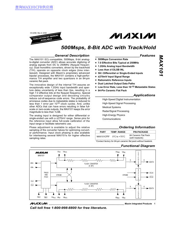
Page 1 Text Content
查询MAX101CFR供应商
19-0296; Rev 0; 8/94
EVALUATION KIT MANUAL
AVAILABLE
500Msps, 8-Bit ADC with Track/Hold
_______________General Description ____________________________Features
The MAX101 ECL-compatible, 500Msps, 8-bit analog- 500Msps Conversion Rate
to-digital converter (ADC) allows accurate digitizing of
7.0 Effective Bits Typical at 250MHz
analog signals from DC to 250MHz (Nyquist frequen-
1.2GHz Analog Input Bandwidth
cy). Dual monolithic converters, driven by the track/hold
(T/H), operate on opposite clock edges (time inter- Less than ±1/2LSB INL
leaved). Designed with Maxim’s proprietary advanced 50Ω Differential or Single-Ended Inputs bipolar processes, the MAX101 contains a high-perfor-
±270m V Input Signal Range
mance T/H amplifier and two quantizers in an 84-pin
Ratiometric Reference Inputs
ceramic flat pack.
Dual Latched Output Data Paths
The innovative design of the internal T/H assures an
exceptionally wide 1.2GHz input bandwidth and aper- Low Error Rate, Less than 10-15 Metastable States
ture delay uncertainty of less than 2ps, resulting in a 84-Pin Ceramic Flat Pack high 7.0 effective bits at the Nyquist frequency. Special
comparator output design and decoding circuitry ________________________Applications
reduce out-of-sequence code errors. The probability of
High-Speed Digital Instrumentation
erroneous codes due to metastable states is reduced to
less than 1 error per 1015 clock cycles. And, unlike High-Speed Signal Processing
other ADCs that can have errors resulting in false full-
Medical Systems
scale or zero-scale outputs, the MAX101 keeps the error
Radar/Signal Processing
magnitude to less than 1LSB.
The analog input is designed for either differential or High-Energy Physics
single-ended use with a ±270m V range. Sense pins for
Communications
the reference input allow full-scale calibration of the input range or facilitate ratiometric use. Phase adjustment is available to adjust the relative ______________Ordering Information sampling of the converter halves for optimizing convert-
PART TEMP. RANGE PIN-PACKAGE
er performance. Input clock phasing is also available
for interleaving several MAX101s for higher effective 84 Ceramic Flat Pack
MAX101CFR* 0°C to +70°C
sampling rates. (with heatsink)
*Contact factory for 84-pin ceramic flat pack without heatsink.
_________________________________________________________Functional Diagram
VART VARTS VARBVARBS
MAX101
ADATA
FLASH CONVERTER (8 -BIT)
TRACK DCLK AND STROBESTROBE HOLD DCLK
FLASH CONVERTER
(8 -BIT)
BDATA
PHADJTRK1TRK1 VBRT VBRTS VBRBVBRBS
Maxim Integrated Products
Call toll free 1-800-998-8800 for free literature.
Page Summary Contents For MAXIM MAX101 500Msps, 8-Bit ADC with Track Hold User Manual Data Sheet
Manual Details
| Brand | ADC |
|---|---|
| Pages | 16 |
| File Size | 152.35 KB |
| Published | May 13, 2026 |
Enter the captcha to get the download link:

Frequently Asked Questions
How can I increase the effective sampling rate using multiple MAX101 units?
Phase adjustment is available to optimize conversion for interleaving several MAX101s and achieving a higher effective sampling rate.
What kind of signal input range does this ADC support?
The analog input design accommodates either differential or single-ended use, offering a maximum range of ±270mV.
Is full-scale calibration of the input possible?
Yes, the dedicated reference input allows for full-scale calibration of the input range or can facilitate ratiometric measurements.
What structural element must be considered for high-speed operation?
The module requires proper thermal management; when operating at certain conditions, a heatsink may be necessary to maintain stable junction temperatures.